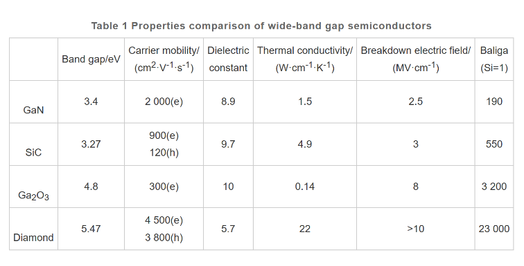
Wide bandgap semiconductor materials and devices have many applications in information, energy, transportation, national defense and other fields, and have become one of the key fields of high-tech competition in the world. As shown in Table 1, compared with GaN, SiC,Ga2O3and other semiconductor materials, diamond has a large band gap (5.47 eV), high carrier mobility [hole (h) mobility of 3800cm2·V-1·s-1, electron (e) mobility of 4 500cm2·V-1·s-1], high thermal conductivity, and high conductivity,making it very suitable for the preparation of high power, high frequency electronic devices.

The metal-oxide-semiconductor field-effect transistor (MOSFET) is widely used in the fields of power switching, electrical energy conversion and logic operation because of its fast switching speed, high input impedance, low power consumption and easy integration.Diamond, with its excellent properties, is expected to produce ultra high power, Super high frequency MOSFETs, and because of its ultra-high thermal conductivity, it can greatly simplify its cooling system and reduce costs.
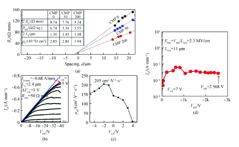
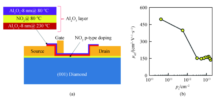
The Chinese team successfully prepared a diamond heterointegration substrate with a size of 26 mm×26 mm×1 mm on the sapphire substrate, and the full width of the half-peak XRD swing curve of the (004) surface is 209.52 arcsec.The maximum source leakage current of the prepared field-effect transistor is -172 mA/mm.The effect of low-temperature annealing on device performance under nitrogen atmosphere was studied. In the same year, Kasu et al. used chemical mechanical polishing (CMP) technology to polish diamond heterointegration substrate to improve surface smoothness and reduce defects.After 200h CMP treatment, the diamond surface roughness is 0.04 nm and the surface block resistance of hydrogen terminal is 3.55 kΩ/sq, as shown in FIG. 1(a). The MOSFET with Al2O3 as the dielectric layer was prepared in the experiment. The maximum drain current density of the device can reach -0.68A /mm(see Figure 1(b)), the maximum effective mobility is 205 cm2/(V·s)(see Figure 1(c)), and the specific on-resistance is 7.54 mΩ·cm2. The breakdown voltage of the device in the off state reaches -2568 V and the breakdown electric field reaches 2.3 MV/cm, which is close to the theoretical critical electric field of GaN and SiC. The BFOM of 874.6MW ·cm-2 is the highest value ever reported, demonstrating the strong potential of diamond in power electronics.

Takeuchi team at 2 mm × 2 mm × Diamond quasi vertical p-i-n diodes were prepared on a 0.1 mm (001) diamond heterointegration substrate. As shown in Figure 2, the current voltage characteristics of the p-i-n diode exhibit good rectification characteristics. Increasing the forward current leads to a sublinear increase in the integrated intensity of defect luminescence, while the integrated intensity of free exciton luminescence increases superlinearly. This significant trend is consistent with the observed trend in p-i-n diodes prepared using homogeneous epitaxial growth films on traditional HTHP synthesized diamond substrates. It indicates the potential of diamond heterointegration substrates in future diamond based electronic devices.

CSMH focuses on the research and production of diamond wafers, and currently has diamond wafer, diamond heat sink , GaN on diamond ,AIN on diamond and other products, providing professional and leading diamond products and solutions for domestic and foreign customers.
 闽ICP备2021005558号-1
Leave A Message