Pos:
Home KnowledgeTechnologyGaN-on-diamond semiconductor material that can take the heat - 1,000℃ to be exactResearchers succeed in the direct bonding of diamond and gallium nitride (GaN) at room temperature and demonstrate that the bond can withstand heat treatments of 1,000℃, making it ideal for the high temperature fabrication process of GaN-based devices. GaN-on-diamond semiconductor material will allow for the next generation of high power, high frequency devices.

A GaN layer epitaxially grown on Si substrate is successfully bonded to a 10-mm by 10-mm diamond plate with no use of intermediate layers. The photo, taken from the transparent diamond side, shows that the entire GaN layer is successfully bonded to diamond.
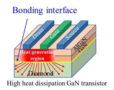
High heat dissipation GaN transistor
The need for more powerful electronic devices in today’s society is curtailed by our ability to produce highly conductive semiconductors that can withstand the harsh, high temperature fabrication processes of high-powered devices.
Gallium nitride (GaN)-on-diamond shows promise as a next-generation semiconductor material due to the wide band gap of both materials, allowing for high conductivity, and diamond’s high thermal conductivity, positioning it as a superior heat-spreading substrate. There have been attempts at creating a GaN-on-diamond structure by combining the two components with some form of transition or adhesion layer, but in both cases the additional layer significantly interfered with diamond’s thermal conductivity – defeating a key advantage of the GaN-diamond combination.

“There is thus a need for a technology that can directly integrate diamond and GaN,” states Jianbo Liang, Associate Professor of the Graduate School of Engineering, Osaka City University (OCU), and first author of the study, “However, due to large differences in their crystal structures and lattice constants, direct diamond growth on GaN and vice versa is impossible.”
Fusing the two elements together without any intermediate layers, known as Wafer direct bonding, is one way of getting around this mismatch. However, to create a sufficiently high bonding strength many direct bonding methods, the structure needs to be heated to extremely high degrees (typically 500℃) in something called a post-annealing process. This generally causes cracks in a bonded sample of dissimilar materials due to a thermal expansion mismatch – this time defeating any chance of the GaN-diamond structure surviving the extremely high temperatures that high-power devices go through during fabrication.
“In previous work, we used surface activated bonding (SAB) to successfully fabricate various interfaces with diamond at room temperature, all exhibiting a high thermal stability and an excellent practicality,” says research lead Professor Naoteru Shigekawa.
As reported this week in the journal ADVANCED MATERIALS, Liang, Shigekawa and their colleagues from Tohoku University, Saga University, use the SAB method to successfully bond GaN and diamond heat sink , and demonstrate that the bonding is stable even when heated to 1,000℃.
SAB creates highly strong bonds between different materials at room temperature by atomically cleaning and activating the bonding surfaces to react when brought into contact with each other.
As the chemical properties of GaN is completely different from materials the research team has used in the past, after they used SAB to create the GaN-on-diamond material, they used a variety of techniques to test the stability the bonding site – or heterointerface. To characterize the residual stress in the GaN of the heterointerface they used micro-Raman spectroscopy, transmission electron microscopy (TEM) and energy-dispersive X-ray spectroscopy shed light on the nanostructure and the atomic behavior of the heterointerface, electron energy-loss spectroscopy (EELS) showed the chemical bonding states of the carbon atoms at the heterointerface, and the thermal stability of the heterointerface was tested at 700℃ in N2 gas ambient pressure, “which is required for GaN-based power device fabrication processes”, states Liang.
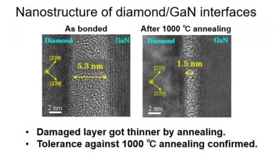
Results showed that at the heterointerface an intermediate layer of approximately 5.3 nm formed that was a mixture of amorphous carbon and diamond in which Ga and N atoms were distributed. As the team increased annealing temperatures, they noticed a decrease in the layer thickness, “due to a direct conversion of amorphous carbon into diamond,” as Shigekawa puts it. After annealing at 1,000℃, the layer decreased to 1.5nm, “suggesting the intermediate layer can be completely removed by optimizing the annealing process,” continues the professor. Although numbers for compressive strength of the heterointerface improved as annealing temperatures increased, they did not match those of GaN-on-diamond structures formed by crystal growth.

However, “as no peeling was observed at the heterointerface after annealing at 1000℃,” states Liang, “these results indicate that the GaN/diamond heterointerface can withstand harsh fabrications processes, with temperature rise in gallium nitride transistors being suppressed by a factor of four.”
 闽ICP备2021005558号-1
Leave A Message