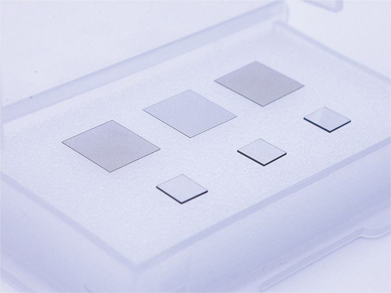
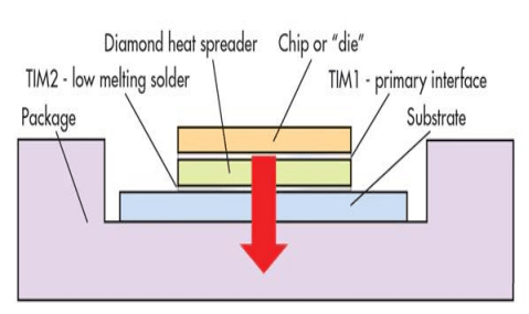
With the increase in power density and reduction in size of GaN based electronic power converters, their heat dissipation performance becomes particularly critical in practical applications. Diamond stands out among all natural materials due to its excellent thermal conductivity (up to 2000W/m.k), making it an ideal choice for integration with GaN to efficiently dissipate the heat generated by AlGaN/GaN high electron mobility transistor (HEMT) channels. At present, the combination process of diamond and GaN is constantly improving. Below, we will outline various technical implementation methods for diamond heat sinks used for GaN heat dissipation in the industry.

Diamond substrate heat dissipation technology:
Diamond on GaN: This method can obtain larger diamond substrate wafers, which helps to reduce costs. However, in order to grow diamond materials on GaN layers, CVD technology above 600 ℃ is generally used to grow on seed crystal layers such as SiN. This method may lead to the appearance of nucleation layers and thermal stress that affect the quality of diamond materials.
GaN on Diamond: Directly epitaxial growth of GaN structures on diamond substrates is a challenging method, as both polycrystalline diamond (PCD) and single crystal diamond (SCD) suffer from poor electrical performance of AlGaN/GaN layers. Therefore, more precise interface control and stress management need to be achieved during epitaxial growth and final cooling processes.
GaN/Diamond bonding: The GaN/Diamond bonding method based on transfer technology is more flexible and serves as a parallel process, The GaN epitaxial layer and diamond substrate can be prepared simultaneously before bonding, making them increasingly attractive for high-power GaN devices. Due to the fact that the early bonding experiments of this technology were generally conducted at a high temperature of 800 ℃, which greatly limited the growth area and required the introduction of low thermal conductivity interface bonding materials, the performance advantages of the device could not be fully utilized.
Researchers removed the silicon substrate from the multi unit GaN HEMT manufactured on the silicon substrate, polished the back of the GaN HEMT to make it thinner and smoother, and then directly bonded it to the diamond substrate using a nano adhesive layer. Its multi unit structure is used for parallel alignment of eight transistor units in actual products. Finally, the world's first multi unit GaN on Diamond HEMT was fabricated using a single crystal diamond high heat dissipation substrate.

Diamond embedded heat dissipation column technology:
Using SiC based GaN devices to deeply etch the SiC substrate in the lower region of its active region, and using growth technology to grow diamond materials on the etching holes, a diamond embedded heat dissipation column structure is achieved, which effectively diffuses heat from the heat source area through the diamond heat dissipation column.
High thermal conductivity passivation layer heat dissipation technology:
Based on traditional SiC based GaN devices, MPCVD growth technology is adopted on both sides of the gate in the active region to grow nanoscale diamond thin film layers, replacing the traditional passive layer SiNX material in the original source region and increasing its lateral heat transfer ability in the heat source region.
CSMH is committed to researching the growth of diamond materials, Its core products include diamond wafers, diamond heat sinks, diamond windows, diamond hetero-integrated composite substrates, etc. Among them, the surface roughness of diamond wafers Ra < 1nm can meet the requirements of bonding materials such as GaN,SiC,etc., the thermal conductivity of diamond heat sinks reaches 1000-2000W/m.K. The products have applications in fields such as optical communication, high-power lasers, drones, 5G base stations, photovoltaics, and new energy vehicles.
 闽ICP备2021005558号-1
Leave A Message