Diamond is an ultra wide bandgap semiconductor material with excellent properties such as high carrier mobility, high carrier saturation drift rate, strong breakdown field, and high thermal conductivity. It is an ideal material for solving the heat dissipation problem of high-frequency and high-power electronic devices. Using diamond wafers as a heat sink/substrate for high-power electrical components can significantly improve the device's heat dissipation ability, effectively improve the high-temperature degradation of the device, and enhance the device's power characteristics.
Traditional GaN power devices generally choose Si, SiC, etc. as substrate materials. In recent years, with the continuous improvement of power device technology, the theoretical output power is getting higher, the frequency is getting larger, and the volume is getting smaller. Relying solely on traditional substrate materials through passive cooling technology is no longer sufficient to meet the heat dissipation requirements under high-power conditions, and has become one of the main bottlenecks limiting the further development of power devices.
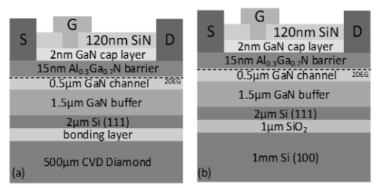
The use of diamond wafers with higher thermal conductivity as the substrate/heat sink for high-frequency and high-power devices has demonstrated excellent performance:
1. High temperature degradation of drain current
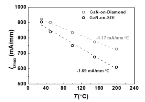
At 200 ℃, the degradation rate based on Si substrate is significantly higher than that based on diamond substrate, indicating a significant improvement in high-temperature degradation of devices using diamond substrate. By using diamond substrates, the device's heat dissipation ability is improved, and the degradation of 2DEG with temperature is effectively suppressed.
2. Power characteristics
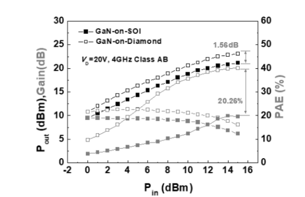
The saturated output power density of the diamond substrate based HEMTs device after transfer is 2.0W/mm, which is 1.56dB higher than the device before transfer. The power additional efficiency (PAE) has doubled compared to the pre transfer device, reaching 40.12%. The improvement in power performance further demonstrates the success of the entire transfer process, and also demonstrates that the modulation of the device's heat dissipation ability after using diamond substrates enhances the power characteristics.
3. Junction temperature change
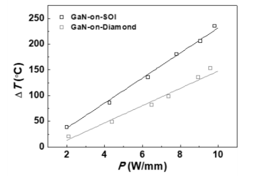
Extract the junction temperature of the device before and after transfer, with a device area of 400 μ m × 400 μ m. It can be observed that under the same dissipation power, the junction temperature of the transferred GaN on Diamond HEMTs device is significantly lower than that of the GaN on SOI HEMTs device. It can be observed that when the DC power consumption reaches 10W/mm, the junction temperature of GaN on SOI HEMTs device reaches 231.6 ℃, while the transferred GaN on Diamond HEMTs are 147.7 ℃, and the junction temperature decreases by 83.9 ℃.
4. Thermal simulation
Establish a thermal simulation model of the sample using finite element software ANSYS, and calibrate the model based on the results of junction temperature testing. The substrate temperature rise in GaN onSOI HEMTs before transfer accounts for 77% of the total device temperature rise, which is the main factor hindering device heat dissipation. The temperature of the transferred GaN on Diamond HEMTs device significantly decreases, with the temperature rise of the diamond substrate accounting for only 17% of the overall temperature rise of the device, while the temperature rise of the bonding layer accounts for 42% of the overall temperature rise of the device, becoming a bottleneck factor affecting the improvement of the device's heat dissipation ability and the key to subsequent process optimization.
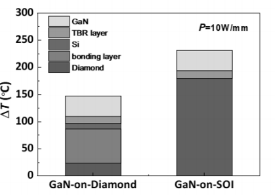
The data shows that power devices using diamond heat sinks/substrates have higher heat dissipation capabilities, which will have extremely high application value in high-power RF, microwave communication, 5G/6G, aerospace, national defense and other fields. CSMH currently has products such as diamond heat sinks, diamond wafers, diamond window chips, diamond based aluminum nitride, diamond and gallium nitride heterointegration. Among them, diamond heat sinks have a thermal conductivity of 1000-2200W/(m.k), making them the preferred substrate material for high-power devices.
 闽ICP备2021005558号-1
Leave A Message