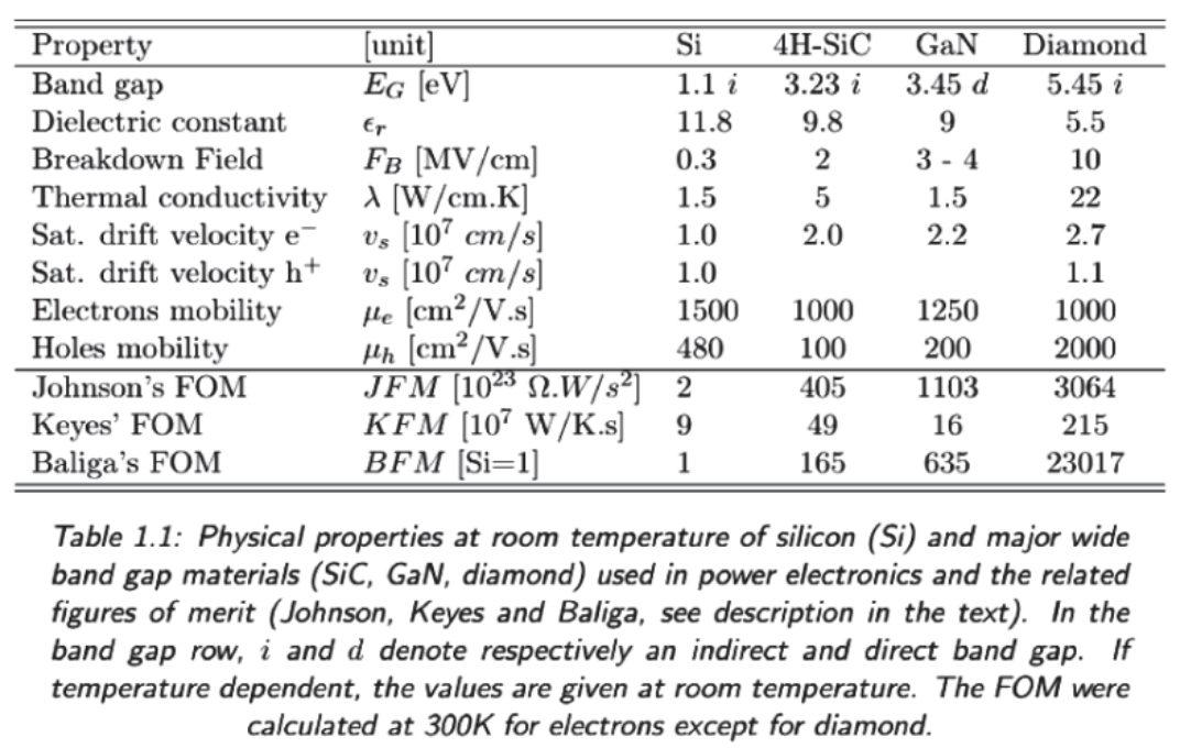
With the development of 5G communication technology and the widespread commercial use of third-generation wide band-gap semiconductors, power electronic devices are accelerating towards high-frequency, miniaturization, and high energy efficiency. Traditional silicon based power devices have been widely used in daily production. However, due to the physical characteristics of silicon materials, existing silicon based power devices always have two defects, namely, they cannot operate at high temperatures (greater than 150 ℃) and cannot withstand high voltages (greater than 10KV). Referring to the table below, it can be seen from the characteristics exhibited by diamond that using diamond to make power devices instead of silicon based power devices will achieve very good results. As shown in Figure, the band-gap width, breakdown field, and thermal conductivity of diamond are far superior to existing silicon based materials.

1. Schottky diode
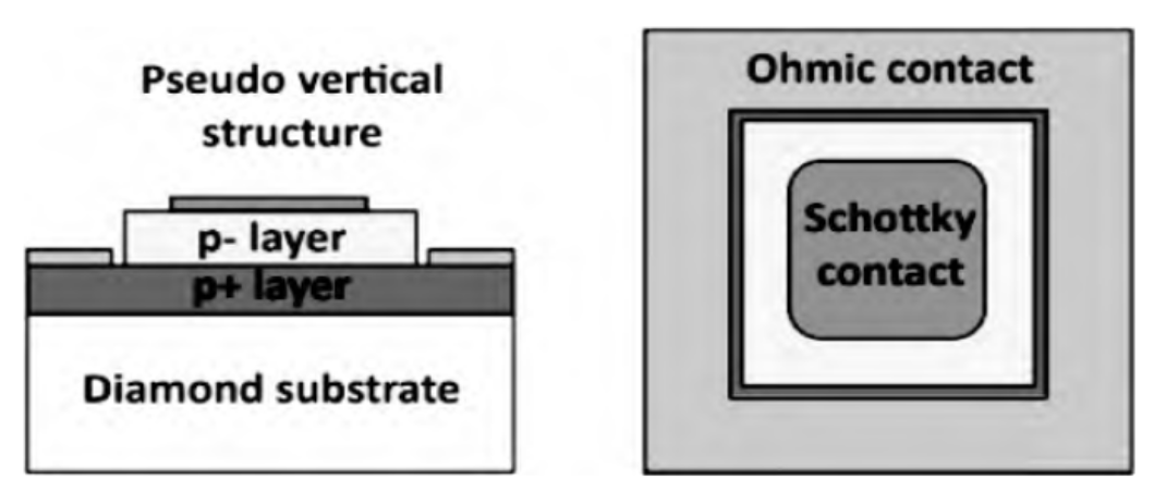
Among various power devices, using diamond to produce Schottky diodes is a very good entry point, because the structure of Schottky diodes is relatively simple, the production steps are not very complex, and p-type doping can refer to more data, which can quickly verify various theories.

2.PiN diode
PiN diode is also a common power diode. The inherent layer and n-doped layer in the middle are challenges in the production process of PiN diodes using diamond materials. The figure shows the configuration and parameters of a diamond PiN diode.

3. Metal oxide Field-effect transistor (MOSFET)
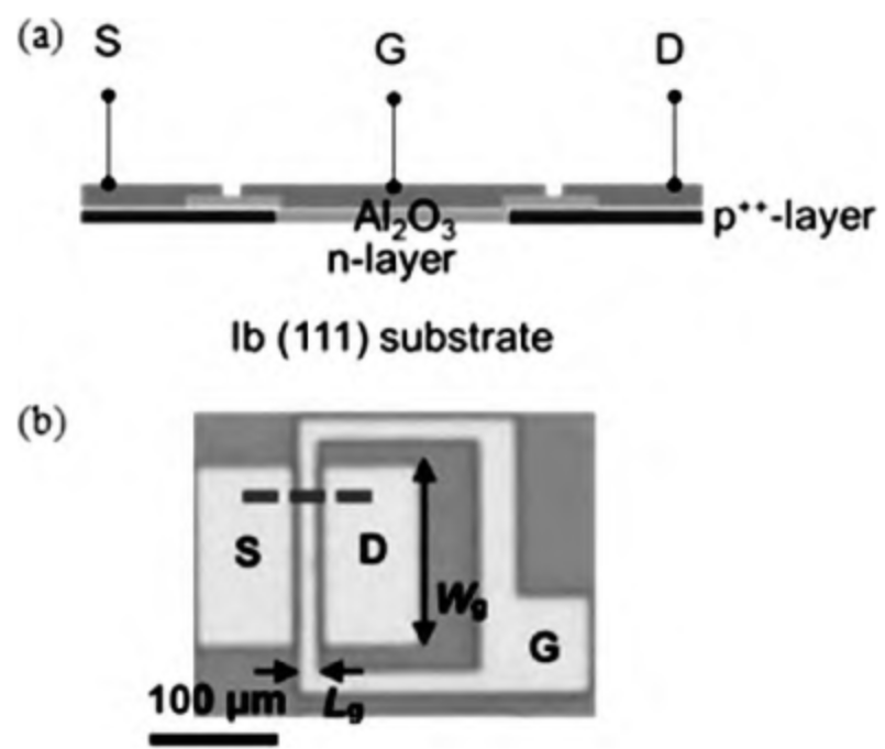
At present, silicon based MOSFET are widely used in electronic products. The use of diamond materials to replace the existing silicon based metal oxide Field-effect transistor will not only bring huge performance improvements to electronic products, but also a breakthrough point to obtain huge market value. The figure is a cross-sectional view of a diamond metal oxide Field-effect transistor. The production process involves growing n-type doped diamond semiconductors on diamond substrates, regenerating highly doped p-type diamond semiconductors, and etching away excess highly doped p-types to leave space for the oxide layer. Use Atomic layer deposition (ALD) to grow oxide layer, and finally cover metal layer to complete device fabrication.

CSMH focuses on the research and production of diamond wafers, and currently has diamond wafer, diamond heat sink , GaN on diamond ,AIN on diamond and other products, providing diamond thermal management solutions for our customers.
 闽ICP备2021005558号-1
Leave A Message