With the continuous development of science and technology, nuclear power plants, space equipment, scientific research and medical radiation devices are the key areas of current development. However, nuclear power plants, space exploration, radiation devices and so on put forward strict requirements on the performance of various nuclear detectors. The traditional semiconductor nuclear detectors made of semiconductor materials such as silicon and germanium can no longer meet the needs of current scientific development, and it is urgent to research and develop new nuclear detectors.
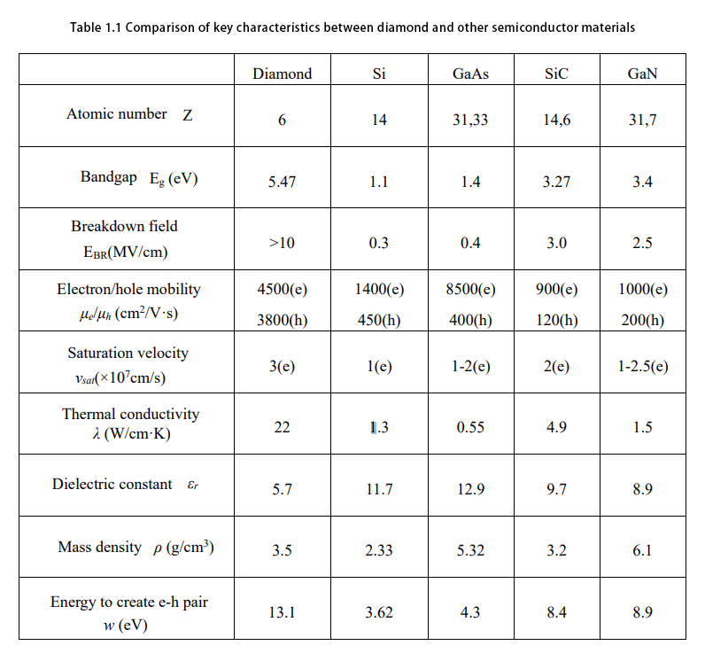
Diamond has excellent physical properties, making it an ideal material for the next generation of strong radiation field nuclear detectors. Table 1.1 lists the comparison results of diamond and other typical semiconductor materials. The atomic number ( Z ) of diamond is 6. The lower atomic number reduces the radiation damage caused by high energy cascade and multiple scattering in high energy physics experiments. Because the atomic number of diamond is close to that of human muscle and tissue ( Z ≈ 7.5 ), it can better reflect the radiation damage characteristics of human body and has better human body equivalence, which is suitable for medical dosimetry measurement. The band gap ( Eg ) of diamond is as high as 5.47 eV, which means that diamond has super anti-radiation characteristics and extremely low intrinsic carrier concentration ( the resistivity of intrinsic diamond is as high as 1016Ω · cm at room temperature ). Diamond can obtain very low dark current, and can show high sensitivity and signal-to-noise ratio for low-intensity radiation. The carrier mobility ( μe ) of diamond reaches 4500 cm2 / V · s ( μe electron ) and 3800 cm2 / V · s ( μe hole ), respectively. The relative dielectric constant ( εr ) of diamond is only 5.7. The parasitic capacitance is only half of that of silicon and 0.6 times of that of silicon carbide at the same size. The ultrafast time response of picosecond level can be obtained, and lower noise can be obtained in the signal readout process. The thermal conductivity ( λ ) of diamond reaches 22 W / (cm · K), which is four times that of conventional heat dissipation material-copper / silver. As a detector material, it can not be disturbed by thermal effect. The ionization energy ( w ) of diamond is larger, and the energy required to produce a pair of electron-hole pairs is larger than that of other semiconductors, but it can be solved by readout electronics system amplification.
In addition to the above material properties, the melting point of diamond is as high as 3550 ~ 4000 ° C, slightly higher than that of tungsten, has the highest Mohs hardness ( 10 ), and the thermal expansion coefficient is only 0.8 × 10⁻⁶ / K. Diamond also has strong chemical inertness and is not subject to acid and alkali corrosion, which means that diamond can withstand harsh environmental shocks. The small volume of diamond hardly affects the radiation field, and the non-toxicity will not cause harm to the human body. Through the above analysis, it can be seen that diamond has obvious advantages over silicon ( Si ), gallium arsenide ( GaAs ), silicon carbide ( SiC ) and gallium nitride ( GaN ) materials, making it an ideal material for future development of nuclear detectors.

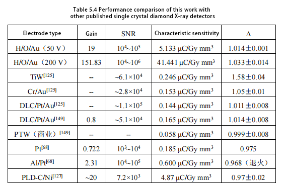
The A index is an important parameter for X-ray dose rate measurement. If = 1, it indicates that the response current of the detector does not change with the change of dose rate, which is very useful for accurate evaluation of absorbed dose. Compared with other published and commercial diamond detectors in Table 5.4, the diamond X-ray detector with this structure has obvious performance advantages due to the good ohmic contact between hydrogen-terminated diamond and Au. The gain, SNR, characteristic sensitivity and A index of the device under 50 V bias are 19,104 ~ 105,5.133 μC / Gy mm3 and 1.014 ± 0.001, respectively. The gain, SNR, characteristic sensitivity and A index of the device under 200 V bias are 151.83, 104 ~ 106, 41.441μC / Gy mm3 and 1.033 ± 0.014, respectively.

CSMH focuses on the research and production of diamond wafers. At present, it has diamond wafers, diamond heat sinks, GaN on diamond, AlN on diamond and other products. Among them, high-power semiconductor lasers packaged by diamond heat sinks have been used in optical communications. In the fields of laser diodes, power transistors, and electronic packaging materials, it can provide customers with diamond thermal management solutions.
 闽ICP备2021005558号-1
Leave A Message