Pos:
Home KnowledgeTechnologySynthesis of nitrogen-doped multilayer homoepitaxial single crystal diamond wafer on diamond substrateIn the present investigation, a nitrogen-doped multilayer homoepitaxial single crystal diamond is synthesized on a high-pressure high temperature (HPHT) Ib-type diamond substrate using the microwave plasma chemical vapor deposition (MPCVD) method. When 0.15 sccm of nitrogen was added in the gas phase, the growth rate of the doped layer was about 1.7 times that of the buffer layer, and large conical and pyramidal features are formed on the surface of the sample. Raman mapping and photoluminescence imaging of the polished cross sectional slice shows a broadband emission, with a characteristic zero phonon line (ZPL) at 575 nm in the doped layers, and large compressive stress was formed in the nitrogen-doped layers. X-ray topography shows that the defects at the interface can induce dislocation. The pyramid feature is formed at the defect, and more nitrogen-related defects are formed in the pyramid region. Thin nitrogen-doped multilayers were successfully prepared, and the thickness of the nitrogen-doped and buffer layers was about 650 nm each. The indentation measurements reveal that the thin nitrogen-doped multilayers are ultra-tough (at least ~22 MPa m1/2), compared to the Ib-type HPHT seed substrate (~8 MPa m1/2) and the unintentionally doped chemical vapor deposition (CVD) single crystal diamond (~14 MPa m1/2).
Graphic analysis
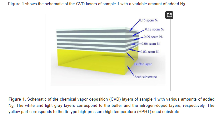
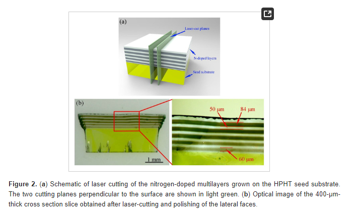
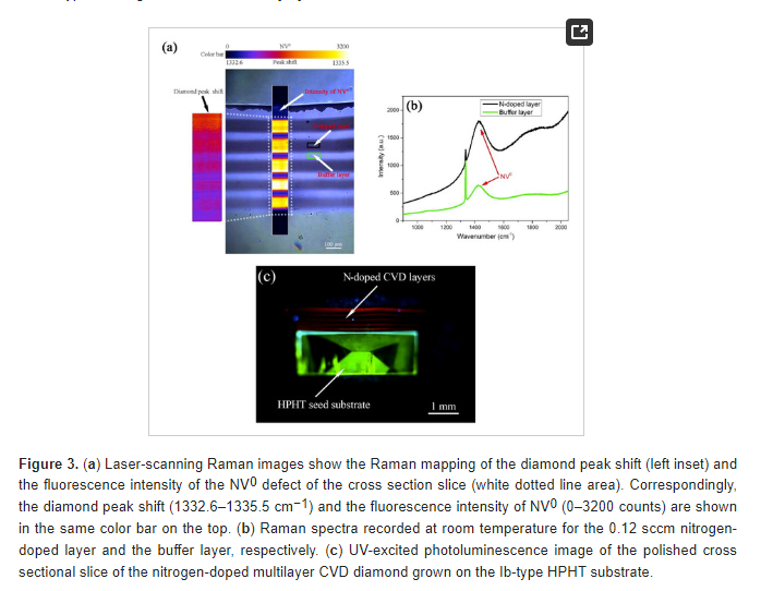
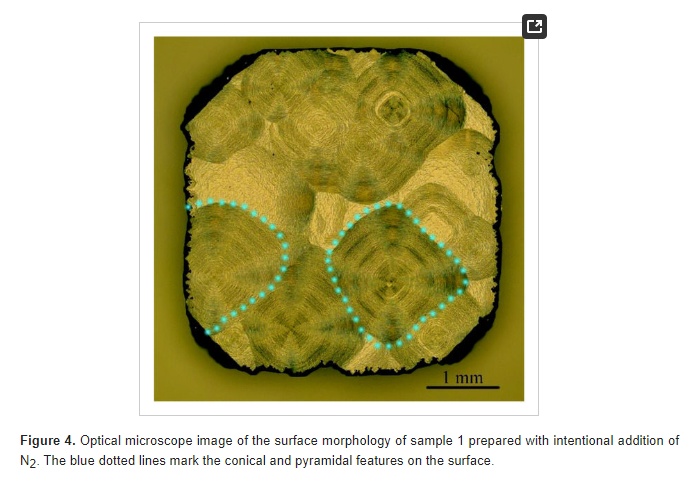
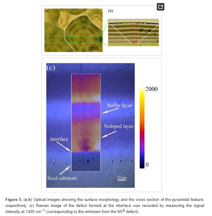
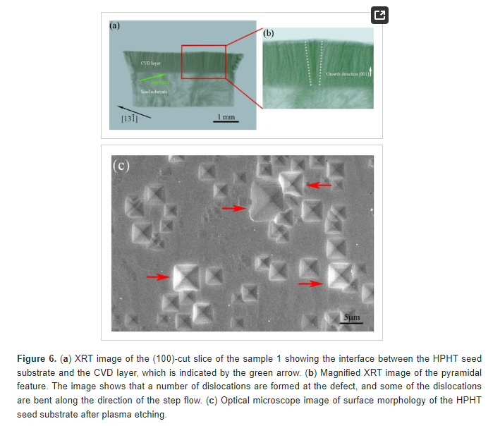
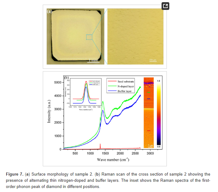
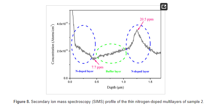
Defects at the interface between the substrate and the epitaxial layer can induce dislocation, and more nitrogen-related defects are included into the pyramidal region. We have succeeded in fabricating thin nitrogen-doped multilayer single crystal diamond on (100)-oriented HPHT seed substrate under high power densities using MPCVD technology. When the thickness of the nitrogen-doped and the buffer layers was about 650 nm each, the fracture toughness of the thin nitrogen-doped multilayer CVD single crystal diamond was much higher than that of the HPHT seed substrate and the unintentionally doped CVD single crystal diamond. Further improvements will include the growth of thinner nitrogen-doped layers. The present study may provide the guidance for the future synthesis of ultra-tough and ultra-hard materials consisting of alternately-stacked and differently nitrogen-doped diamond layers. This method induces novel toughening and hardening of CVD single crystal diamonds.
CSMH has made breakthroughs in the three combination schemes of GaN & Diamond. The existing diamond heat sinks for GaN on Diamond, Diamond on GaN and GaN & Diamond bonding are world-class. The technical indexes of electro-deposited diamond heat sink and wafer-level diamond products have reached the world 's leading level. The surface roughness of wafer-level diamond growth surface is Ra < 1nm, and the thermal conductivity of diamond heat sink is 1000-2200W / m.K.
 闽ICP备2021005558号-1
Leave A Message