Pos:
Home KnowledgeTechnologyDiamond wafers for high-power high-temperature, high-voltage, high-frequency electronic equipmentDiamond is a hopeful candidate material for next generation power devices due to its favorable properties such as a high breakdown field, high thermal conductivity, high mobility and low dielectric constant. Diamond wafers are far better than Si materials in terms of output power, operating temperature, and operating frequency. Regardless of output power or operating frequency, diamond devices are superior to other devices, and are the most potential high-frequency high-power electronic devices. With the growth of high-quality semiconductor diamond material by MPCVD method, diamond wafers are used in more and more fields.

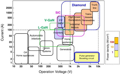
Fig. 1. Application possibilities in current- voltage map.
Firstly, we predict applications for diamond devices in the high voltage field, such as high power generators and inverters for trains, ships, renewable energy systems, and power trunk line systems. The realization of SiC unipolar devices using both SBD and MOSFET for high voltage applications enabled low loss devices compared to previous Si bipolar devices. This is due to the accumulation and recombination of minority carriers in the bipolar device, whereas the charge transfer in unipolar devices only depends on the depletion and transferred charges. In the higher voltage region, wide bandgap bipolar devices suffer high forward loss of Von × Ion, due to high “on voltage” such as over 4 V for SiC. Hence, diamond unipolar devices with low losses might find applications in the high voltage field.
Another important factor that allows SiC devices to realize low losses is the fast switching or high frequency operation, typically several micro-seconds . This fast switching enables electric power regeneration during the high speed running mode of trains that avoids using the mechanical break system. Low loss unipolar diamond power devices may have faster switching compared to SiC devices; this has been partly verified by SBD. Additionally, fast switching also implies smaller power module with small size capacitor C and reactor L of high frequency operation. A total volume reduction for SiC module of 55% can be attained compared to Si IGBT and pn diode modules .
For extremely high voltage applications over 10 kV device, wide bandgap bipolar devices are expected to open up new opportunity in the future , diamond bipolar devices are a hopeful candidate owing to their favorable characteristics. Diamond that uses deep energy level carriers has increased numbers of carriers at high temperature. The tradeoff in carrier increases with the mobility decrease brought by “carrier scattering”, resulting in a constant current between 150 and 250 °C . This characteristic has inspired new type of high output power device module operating at self-heating temperatures; which are thermally insulated without cooling. In addition, there exist numerous applications in lower voltage range including ultra and super high frequency fields. Here, AlGaN/GaN HEMT devices are already used for many applications incorporating high mobility two dimensional electron gas (2DEG) channel.

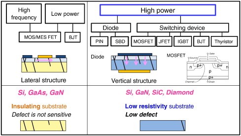
Fig. 2. Device applications and corresponding device structures and wafer.
Some applications and their corresponding device structures are shown in Fig.2. For the low power devices including high frequency applications, the lateral structure is adopted for the devices such as field effect transistors (FET). AlGaN/GaN HEMT power devices are commercialized for high frequency application using insulating substrates. Dislocations are not critical for this application, because of the lateral current flow. On the other hand, the vertical structure is adopted for high power applications to meet the requirements for high current densities. In the vertical structure, current flows from the substrate surface to the electrode at the back surface, thus the majority of the substrate acts as a resistive power loss layer and simultaneously a thermally resistive layer. In order to fabricate low loss devices for high power devices, a low resistivity substrate is essential, often requiring a final back-lap process to thin the substrate.
CSMH has mastered the core process of preparing high-quality diamond by MPCVD and realized mass production. Using special grinding and polishing equipment, the surface roughness of the CVD diamond growth surface is Ra < 1 nm, mirror-like luster, and the thermal conductivity of the diamond wafer is 1000-2000W. /m.k. It fully conforms to the extremely low surface roughness and extremely high surface precision that diamond needs to have as an electronic component, thereby increasing the contact area and improving its heat dissipation efficiency.
High-power semiconductor lasers using diamond heat sinks have been used in optical communications, and are also used in laser diodes, power transistors, and electronic packaging materials. Based on diamond wafer product capabilities, the company has developed GaN-on-diamond epitaxial wafers, which are mainly used in radio frequency (satellite, 5G base station) and high-power devices (photovoltaic, wind power, new energy vehicles, energy storage) and other Areas with high thermal management needs, as a complement to GaN-on-SiC materials.
 闽ICP备2021005558号-1
Leave A Message