Pos:
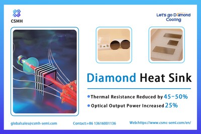
Home NewsCompany ProfileDevelopment, Properties, and Applications of Diamond Wafer Based Heat SinksHeat sink is an essential component to nanoelectronics, microelectronics, and optoelectronics applications because it allows the thermal management of devices such as integrated circuits (ICs), microelectromechanical systems (MEMSs), and graphic unit processing. There are different materials being employed for heat sink production. Among them, diamond has stood out due to its excellent chemical and physical properties.
Laboratory-grown CVD diamond has been extensively studied, not only for its exceptional set of properties but also because the CVD method exceeds limiting barriers for exploration niches in science and industry. This technology is based on the metastability of the crystalline phase of carbon and diamond, under certain environmental conditions. By using a mixture of hydrocarbon gas in excess of hydrogen gas under pressures below of atmospheric, with an energy source for gas dissociation and subsequent reaction, carbon condensate to solid state enabling diamond crystals growth and then multiple growth nuclei coalescence form a continuous film over a surface.
As a brief summary of some applications in CVD technique, we have heat sinking components, such as but not limited to transistor high power devices and high power laser diodes.Statistically, reducing the operating junction temperature by 10°C can double a device lifetime. CVD diamond outperforms today's common materials for thermal management, such as copper, silicon carbide, and aluminium nitride, by factors of 3 to 10 times. With the excellent properties such as low weight, electrical insulation, mechanical strength, low toxicity and low dielectric constant, CVD diamond is the optimal heat spreader for device and package designers.
Many deposition methods have been developed since its first report in academia by Derjaguin and Fedoseev in 1975, between the most used methods to grow diamond at low pressures from hydrocarbon gas hot filament, and microwave plasma activation techniques are the ones chosen for either cost efficiency and low complexity apparatus or higher quality films and better growth rates.
Diamond and its laboratrial synthesis have been extensively studied and improved in the last decades. As diamond becomes more feasible as an engineering material, many industrial and technological uses begin to be economically attractive. CVD diamond polycrystalline films already reached all the properties of perfect IIa single crystal diamonds. Taking this into account, CVD diamond is still a better heat management material when compared to conventionally applied metals, and can be used in different levels of quality and physical properties to match specific application demands.
CSMH focuses on the R&D with excellent independent innovation capabilities and more than ten years of technology accumulation. Products including: diamond wafers, diamond heat sinks, GaN-on-diamond epitaxial wafers, aluminum nitride films and piezoelectric materials. The surface roughness of the diamond wafergrowth surface is Ra<1nm, and the thermal conductivity of the diamond heat sinks could be customized from 1000-2000W/m.k.

 闽ICP备2021005558号-1
Leave A Message