Pos:
Home KnowledgeTechnologyRevolutionary Applications of Diamond Heat Sinks in Thermal Management for Advanced PackagingWith the rapid development of technologies such as 5G communications, artificial intelligence, high-performance computing and electric vehicles, the power density of electronic devices continues to increase, and the heat generated by chips grows exponentially. Traditional thermal management materials can no longer meet the heat dissipation requirements of advanced packaging technologies, making thermal management a key bottleneck restricting the performance improvement of electronic devices. Against this backdrop, diamond heat sinks, leveraging their exceptional physical properties, are sparking a material revolution in the field of thermal management for advanced packaging.

Advanced packaging technologies significantly enhance device functional density and interconnection efficiency by stacking and integrating multiple chips in 2.5D/3D configurations, yet they also bring unprecedented thermal management challenges. As the feature size of chips shrinks continuously to the nanoscale, the power consumption per unit area surges sharply, leading to high heat concentration in tiny spaces. In traditional packaging structures, the thermal conductivity of thermal interface materials (TIMs) is usually only 1–5 W/m·K, while the temperature of hotspots inside chips can exceed 150℃, which seriously impairs device performance and reliability. Therefore, the development of heat dissipation materials with ultra-high thermal conductivity has become an urgent demand for the advancement of advanced packaging technologies.
Diamond is the material with the highest known thermal conductivity in nature. It also boasts high thermal stability (able to withstand temperatures above 600℃ in air), low coefficient of thermal expansion (approximately 1×10⁻⁶/K), excellent electrical insulation and chemical inertness, making it an ideal choice for thermal management in advanced packaging.
1. Diamond Thermal Interface Materials (TIMs)
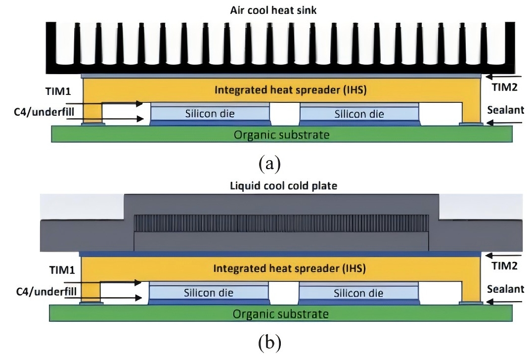
Thermal interface materials serve as the critical bridge connecting chips and heat sinks, and their thermal conductivity directly affects the overall heat dissipation efficiency. Traditional polymer-based TIMs typically have a thermal conductivity of less than 5 W/m·K. By filling high-purity diamond micro-powders or nanoparticles into polymer matrices, the thermal conductivity of the composite materials can be significantly enhanced. Composite materials synergistically filled with surface-functionalized nanodiamond particles (with a particle size of 50–100 nm) and high-quality graphene sheets exhibit a thermal conductivity of 30–50 W/m·K, which is an order of magnitude higher than that of traditional TIMs. Such composite TIMs achieve high thermal conductivity at a low filling rate (<20 vol%) while maintaining good processability and mechanical flexibility.
2. Diamond Heat Dissipation Substrates
For power devices and radio frequency (RF) devices, diamond substrates can be directly integrated beneath chips to form efficient heat dissipation channels.
GaN-on-Diamond: Epitaxially growing a GaN layer on single-crystal diamond via chemical vapor deposition (CVD) forms a direct bonding structure with extremely low interfacial thermal resistance. Experimental data shows that compared with traditional SiC substrates, diamond substrates can reduce the channel temperature of GaN HEMT devices by 40–60%.

Diamond Heat Dissipation Layer Transfer Technology: Transferring high-quality CVD diamond films (with a thickness of 50–300 μm) to the backside of chips through metallization bonding processes to serve as efficient heat dissipation and diffusion layers. This technology is compatible with existing semiconductor processes and applicable to various semiconductor materials such as Si, SiC and GaAs.
3. Diamond Interconnections and Through-Diamond Vias (TDVs)
In 2.5D/3D advanced packaging, diamond can be used to fabricate vertical through-diamond vias (TDVs), effectively addressing the heat dissipation challenge of intermediate chips. By preparing high-density micro-vias in diamond layers and filling them with high-thermal-conductivity metals (e.g., copper), efficient heat dissipation channels running through the entire package are formed, which directly conduct the heat generated inside stacked chips to external heat dissipation devices.
Research data indicates that diamond thermal via arrays with a diameter of 10 μm and a pitch of 50 μm have an equivalent thermal conductivity of 600–800 W/m·K, which is more than 10 times higher than that of traditional through-silicon vias (TSVs), while occupying 60% less area.
4. Diamond Substrates and Interposers
As the interconnection density of chips continues to rise, the thermal management capability of packaging substrates and interposers has become crucial. With its high thermal conductivity and low dielectric constant (ε_r≈5.7), diamond can be used as a high-performance packaging substrate material:
Diamond-Metal Composite Substrates: Diamond-copper/diamond-aluminum composite substrates prepared via powder metallurgy or infiltration processes have a thermal conductivity of 400–800 W/m·K, and their coefficient of thermal expansion is adjustable (5–10×10⁻⁶/K), which matches well with common semiconductor materials.
Diamond Interposers: In 2.5D packaging, diamond interposers not only provide high-speed interconnections between chips but also act as efficient heat dissipation platforms, uniformly distributing and rapidly dissipating the heat generated by multiple chips.
With its exceptional physical properties, diamond is redefining the technological boundaries of thermal management for advanced packaging. From thermal interface materials to heat dissipation substrates, from thermal vias to substrate interposers, diamond offers a revolutionary solution to address the increasingly severe chip heat dissipation challenges.
As the global semiconductor industry’s demand for high-efficiency heat dissipation solutions grows increasingly urgent, diamond, the "ultimate heat dissipation material", boasts broad application prospects. Its industrialization process will not only reshape the landscape of advanced packaging technologies but also potentially spawn brand-new device architectures and application paradigms, injecting strong impetus into the development of the entire electronic information industry.
CSMH uses the MPCVD method to prepare large-sized and high-quality diamonds,and currently has mature products such as diamond heat sinks, diamond wafers, diamond windows,diamond composite materials,etc.Among them,the thermal conductivity of diamond heat sinks is 1000-2200w/(m.k), which has been applied in aerospace, high-power semiconductor lasers, optical communication, chip heat dissipation, nuclear fusion and other fields.
 闽ICP备2021005558号-1
Leave A Message