Pos:
Home KnowledgeTechnologyHeterogenous Integration of Boron-Doped p-Diamond with Monolayer n-MoS2 for PN Junctions Operating at Room TemperatureDiamond holds great potential for power electronics due to its exceptional thermal conductivity, large electric field strength, and high carrier mobility. However, the lack of reliable n-type transport at room temperature has limited the development of diamond-based electronics. Despite considerable effort in n-type doping, n-type diamond devices exhibit high resistance at room temperature and require high temperatures for effective operation due to the large carrier activation energies of phosphorus and nitrogen as n-type dopants. In contrast, diamond has been successfully doped with boron impurities (p-type) via various techniques, with concentrations ranging from 1015cm-3to 1021cm-3. Therefore, integrating atomically thin n-type two-dimensional materials as pseudo-delta-doped layers onto three-dimensional surfaces has recently shown great potential for achieving complementary device operation.

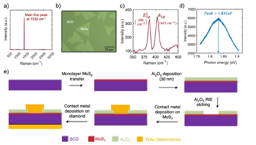
In the experiment, a p-type single crystal diamond (SCD) substrate was used, and its surface quality was evaluated by Raman spectroscopy and atomic force microscopy (AFM). Subsequently, a single layer of MoS₂grown by CVD was transferred to a diamond substrate, and the high quality of MoS₂was confirmed by Raman spectroscopy and photoluminescence (PL) spectroscopy. In order to prepare a 2D/3D heterostructure PN junction diode, the researchers uniformly deposited a 30-nanometer Al₂O₃passivation layer on MoS₂, and then selectively etched the Al₂O₃ layer using DRIE technology to expose MoS₂. Finally, titanium (20 nanometers) and gold (50 nanometers) were deposited as electrodes on p-type diamond and n-type MoS₂, respectively, using photolithography technology. To improve the performance of the diode, the researchers performed a vacuum annealing treatment at 250°C. Experimental results show that this 2D/3D heterostructure diode exhibits excellent rectification characteristics at room temperature, with a maximum forward current density (Jᴅ) of approximately 4000 A/cm², a rectification ratio (RR) of 10⁶, and an ideality factor (η) of approximately 3.7.
Excellent room-temperature rectification properties: A maximum forward current density (Jᴅ) of approximately 4000 A/cm², a rectification ratio (RR) of 10⁶, and an ideality factor (η) of approximately 3.7 were achieved at room temperature.
Unveiling the tunneling mechanism: Experiments and simulations revealed the role of direct tunneling (DT) and Fowler-Nordheim (FN) tunneling mechanisms in current rectification.
Vacuum annealing: Vacuum annealing at 250°C further enhanced diode performance, reduced defect concentration, and improved crystallinity.
A 2D/3D heterostructure PN junction diode was developed by integrating a monolayer of n-type MoS₂ with boron-doped p-type single-crystal diamond. This diode exhibits excellent rectification characteristics at room temperature, with a maximum forward current density (Jᴅ) of approximately 4000 A/cm², a rectification ratio (RR) of 10⁶, and an ideality factor (η) of approximately 3.7. Research indicates that the current rectification originates from the recombination of majority carriers between the layers driven by direct tunneling (DT) and Fowler-Nordheim (FN) tunneling mechanisms. Vacuum annealing at 250°C further improved the diode's performance. This achievement opens new avenues for the development of diamond-based power electronics through integration with two-dimensional materials.
The boron-doped single-crystal diamond produced by CSMH can achieve doping from low concentration to high concentration. It has realized a uniform and controllable concentration and a customizable boron doping process.CSMH uses the MPCVD method to prepare large-sized and high-quality diamonds,and currently has mature products such as diamond heat sinks, diamond wafers, diamond windows,diamond hetero junction integrated composite substrates,etc.
 闽ICP备2021005558号-1
Leave A Message