Micro-electromechanical systems(MEMS)and nanoelectromechanical systems (NEMS) provide ample sensing opportunities. Due to the small dimension, low stiffness and high operating frequencies, excellent attributes and resolutions of mass change and force investigations can be achieved. For characterization of surface properties at the nanoscale, atomic force microscope (AFM) has been widely used. Since the AFM and its applications are based on the interaction between an extremely sharp probe and the sample, the probe surface is one of the crucial concerns. Moreover, characterization at the nanoscale based on the electrical conductivity and the absence of an electronic surface barrier is beneficial. Scanning tunnelling microscopy (STM) and conductive atomic force microscopy (C-AFM) with locally performed C-AFM current–voltage measurements and Kelvin probe force microscopy(KPFM) are the most effective surface analysis methods with atomic- or nanometre-scale spatial resolution requiring high conductivity probes.

Moreover, diamond-coated tips are attractive for nanosensing application because they have remarkable electrochemical features which consist of chemical stability, a wide electrochemical window and high anodic stability. B-NCD achieves semi-metallic conductivity using in situ boron doping in chemical vapourdeposition (CVD) process. Boron-doped diamond films are commonly used as an electrode material for utilization with hazardous organic compounds or sensing applications. Moreover, due to its biocompatibility, it is a great material for sensing various kinds of proteins or DNA .
In this work, experimental investigation of the undoped and boron-doped diamond thin films on cantilevers is presented. Diamond-coated cantilevers are attractive tools for micro- and nanoscale measurements and instrumentation where biological and chemical inertness are required.
The use of truncated cone-shaped substrate holder enabled to grow thin fully encapsulated B-NCD with a thickness of approx. 60 nm and RMS roughness of 17 nm. The surface morphology (crystallite size and roughness decrease) and the molecular structure of diamond films (sp2 rich area at the inter-grains regions) were modified by boron doping.
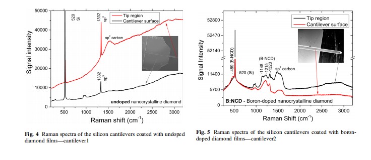
The B-NCD results in high conductivity coverage of cantilever with surface resistivity of 30 m X cm and typical boron-doped nanocrystalline diamond line at 1148 cm-1 recorded by Raman spectroscopy.
The AFM topography showed that crystallite–grain size was 153 nm and 238 nm for boron-doped film and undoped, respectively. The KPFM studies revealed the reasonable decrease in CPD for boron-doped films comparing to an undoped one. Based on CPD values, the values of work functions were calculated as 4.65 eV and 5.15 eV for doped and undoped diamond film, respectively. This fact proves that boron doping increased the carrier density, the conductivity and consequently the Fermi level. Moreover, we have noted that the B-NCD coating changed both resonance frequency and spring constant of cantilever.
Surface modification of the micro- and nanocantilevers is a very interesting opportunity to change mechanical, electrical and physical properties of these micro- and nanodevices. Modified cantilevers can be attractive tools in atomic force microscopes (AFM) as scanning probes in biosensor applications.
The boron-doped single-crystal diamond produced by CSMH can achieve doping from low concentration to high concentration. It has realized a uniform and controllable concentration and a customizable boron doping process.CSMH uses the MPCVD method to prepare large-sized and high-quality diamonds,and currently has mature products such as diamond heat sinks, diamond wafers, diamond windows,diamond hetero junction integrated composite substrates,etc.
 闽ICP备2021005558号-1
Leave A Message