Globally, 6-inch and 8-inch wafers mainly serve the fields of power semiconductors, radio frequency devices, and sensors, which are exactly the stage for third- and fourth-generation semiconductor materials such as silicon carbide (SiC), gallium nitride (GaN), and diamond.
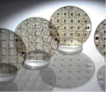
Over the past two decades, wafer sizes have evolved from 4-inch to 6-inch, then to 8-inch and 12-inch. The advantages of size enlargement are straightforward: more chips can be manufactured in the same production batch, reducing costs per unit and improving production efficiency.
Silicon Carbide (SiC): The mainstream mass-production size has transitioned from 4-inch to 6-inch, while 8-inch is being rapidly deployed. From 2020 to 2024, the sales of 6-inch epitaxial wafers grew from $300 million to $800 million, with a compound annual growth rate (CAGR) of 29.5%. The market size of 8-inch wafers is rising quickly, reaching $312 million in 2024, with a CAGR of 186.3% from 2020 to 2024. Manufacturers such as Infineon and Wolfspeed have already laid out 8-inch SiC wafers, which are expected to become the industry mainstream around 2026, though yield improvement remains a bottleneck.
Gallium Nitride (GaN): Initially dependent on 6-inch silicon-based epitaxy, some manufacturers now mass-produce on 8-inch wafers and are exploring the 12-inch route. However, cost control and epitaxial defect management remain challenges.
Diamond: Currently, it is still in the stage of R&D and small-batch production with 2-4 inch sizes. Constrained by large-size single-crystal growth technology and high costs, once these bottlenecks are broken, it may directly leap into high-power devices and high-frequency communication fields.
For new materials like SiC, GaN, and diamond, however, size upgrading is not just a matter of "enlargement". It also comes with technical challenges such as yield rate, defect density, warpage, and thermal stress. The biggest challenges brought by larger wafer sizes include yiel.
 闽ICP备2021005558号-1