Pos:
Home KnowledgeTechnologyMolecular dynamics study of thermal transport across Ga2O3-diamond interfacesβ-Ga2O3 has an ultra-wide bandgap of 4.8 eV, a corresponding breakdown field of about 8 MVcm-1 as well as a greatly higher Baliga figure of merit, the metric for vertical power devices, compared to SiC or GaN. As such, it is an attractive material for potential application in ultra-high voltage electronics—even in excess of 10 kV. A major concern for its implementation in devices remains the material’s low thermal conductivity, which is anisotropic and reaching only 27Wm-1K-1 along the [010] axis, as overheating may result in device failure. Because of this, current research explores the integration of β-Ga2O3 with higher thermal conductivity substrates for better device thermal management. For instance, direct attachment of β-Ga2O3 to diamond via van der Waals bonding has been achieved for the purpose of a photodiode p–n junction. The effects of the orientation of the β-Ga2O3 crystal on the thermal transport across the interface, however, have not been explored. Other attempts at integrating gallium oxide with higher thermal conductivity substrates rely on adhesion via a thin interlayer, such as SiO2 or Al2O3. Such interlayers are known to be necessary when growing diamond on a gallium oxide substrate and β-Ga2O3–diamond superjunctions with Al2O3 interlayers have been considered. Furthermore, there is evidence that the stronger bonding leads to a significant reduction in thermal boundary resistance (TBR) between Ga2O3 and other materials.
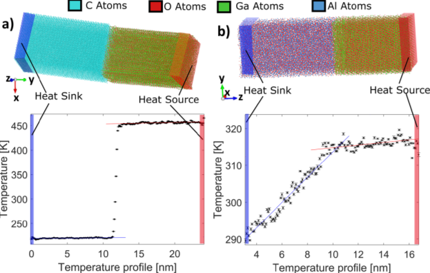
Here, we perform simulations to study the thermal properties of β-Ga2O3 along three main crystallographic axes, investigating how thermal conductivity varies with Ga2O3 layer thickness for different crystal orientations. We estimate the TBR across interfaces to van der Waals bonded diamond and to ionicly bonded amorphous Al2O3 for the (100), (010), and (001) faces of β-Ga2O3. We, thus, help identify the optimal crystallographic orientations of β-Ga2O3 favorable for different device concepts.

 闽ICP备2021005558号-1
Leave A Message