Pos:
Home KnowledgeTechnologyAs the fourth generation of ultra-wideband semiconductors, how important is diamond wafer?Whenever we talk about this problem, we have to say, how to divide the semiconductor era? Then, listen to me: the division of the semiconductor era is divided according to the launch time of semiconductor materials. The first generation began with the invention of integrated circuits, the first transistors were germanium materials, and later developed into silicon materials. The second generation of semiconductor materials, invented and applied in the 80s of the 20th century, mainly refers to compound semiconductor materials, represented by gallium arsenide (GaAs) and indium phosphide (InP). Among them, gallium arsenide plays an important role in RF power amplifier devices, and indium phosphide is widely used in optical communication devices. The third generation of semiconductor materials, proposed after 2000, is mainly based on gallium nitride and silicon carbide. After 2005, ultra-wide bandgap semiconductors began to appear, mainly diamond and gallium oxide.
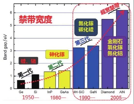
Figure 1 Development history of broadband semiconductors
The industry generally refers to semiconductor materials with bandgap widths greater than 2.3 electron volts (eV) as wide bandgap semiconductor materials. At present, silicon carbide (SiC), gallium nitride (GaN), zinc oxide (ZnO), diamond (C), aluminum nitride (AlN) and other emerging semiconductor materials with wide bandgap (Eg>2.3eV) characteristics, widely used in the production of high temperature, high frequency, high power and radiation-resistant electronic devices, used in semiconductor lighting, 5G communications, satellite communications, optical communications, power electronics, aerospace and other fields, has been considered as a new driving force for the development of today's electronics industry. Among them, ultra-wide bandgap semiconductors such as diamond and gallium oxide are also known as fourth-generation semiconductors.
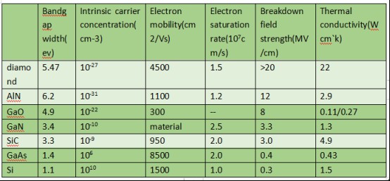
Figure 2 Comparison of the characteristics of several broadband semiconductors
Since the coefficient of thermal expansion (7.2×10⁻⁶/°C) and dielectric constant (9.7) of Al2O3 are high compared to Si single crystals, the thermal conductivity (15-35W/ (m·K)) is still not high enough, resulting in Al2O3 ceramic substrates not suitable for use in 5G high-power electronic devices. The thermal conductivity of SiC ceramics is very high, and the higher the purity of SiC crystallization, the greater the thermal conductivity. The biggest disadvantage of SiC is that the dielectric constant is too high, and the dielectric strength is low, which limits its high-frequency application and is only suitable for low-density packaging; AlN material has excellent dielectric properties and stable chemical properties, but the thermal conductivity is currently only up to 260W/ (m·K), with the accelerated development of electronic products in the direction of high power, high integration, thinning and intelligence, the requirements for heat dissipation are getting higher and higher, and AlN materials also have certain development bottlenecks. Diamond wafer thermal conductivity can be as high as 2000 W/(m.K), thermal expansion coefficient is about 1.1×10⁻⁶/°C, in semiconductor, optics and other aspects of other heat dissipation materials can not achieve excellent characteristics.
Diamond optoelectronic devices: In a diamond crystal, carbon atoms form covalent bonds with four other carbon atoms in sp3 hybrid orbitals to form a tetrahedron, and all valence electrons participate in the formation of co valent bonds. Diamond is not only hard, has a high melting point, is highly transparent, but also does not conduct electricity. In addition, diamond provides the widest optical transparency of naturally occurring materials, extending from the UV region (~225 nm) to terahertz (THz) frequencies and even the microwave region (~8000 μm), where it has low group velocity dispersion, making it suitable for the fabrication of integrated photonics devices.
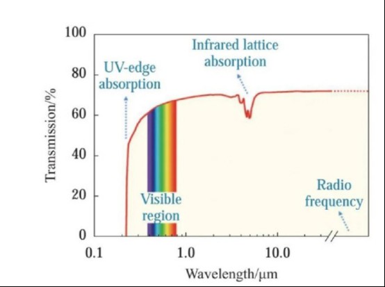
Fig.3 Relationship between diamond crystal wavelength and transmission efficiency
Military infrared window: diamond is expected to have many military uses in the future because of its excellent properties such as high hardness, strong thermal conductivity and infrared light transmittance. Such as missile fairings for thermal shock resistance and high temperature resistance; Infrared optical window with high infrared transmittance and low laser refractive loss; High strength, high hardness and other properties can be used for individual soldier body armor and outer protective layers such as tanks and ships, and diamond has a large application space in the military.
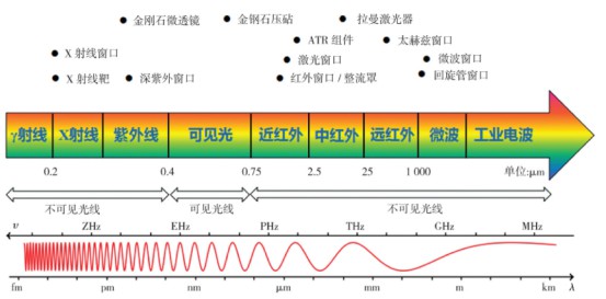
Figure 4 Different optical components reported based on different properties of diamonds
Diamond quantum technology: The ultra-wide band gap of diamond enables the luminescence of deep energy level defects located in the forbidden band to be emitted without being absorbed, forming a series of defect-induced color centers, the so-called "color center". In particular, vacancy-related defects in diamonds, such as nitrogen vacancies (NV) or silicon vacancies (SiV) centers. These color centers have discrete energy levels similar to "single atoms" and are well suited for use in quantum information processing and quantum computing. The strong covalent bond structure of diamond provides a very stable lattice environment for the defect center, so that the defect center has stable optical properties and long spin coherence time, which has important application value in precision measurement. At present, the main research directions are: using diamond as a qubit to prepare quantum information devices (such as quantum computers), using nitrogen vacancy defects in diamond as the "quantum relay node" of quantum networks, and applying them to quantum communication; and diamond magnetic field sensor technology, used in detectors, etc.
Diamond acoustic devices: With its excellent acoustic characteristics, diamonds are efficiently used in high-fidelity speakers, surface acoustic wave devices, acoustic sensors, etc. Among all natural and synthetic materials, diamond has the highest elastic modulus, the fastest sound propagation rate, the highest hardness, low density, good sound damping characteristics, low specific gravity, high fidelity, excellent high-frequency response characteristics, and diamond has high thermal conductivity, which is conducive to dissipating the heat generated by the voice coil to the space through the diaphragm, thereby improving the input power that the speaker can withstand, avoiding burning the voice coil or changing the speaker impedance due to long-term high power input, affecting the accuracy of sound positioning. Therefore, diamond is the best material for the tweeter membrane of high-fidelity speakers.
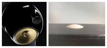
Figure 5 Acoustic application of diamond
CSMH is a high-tech enterprise focusing on the research and development and production of third-generation (wide bandgaping) semiconductor substrate materials and devices, and is committed to becoming the world's leading wide bandgap semiconductor materials and device company. We have always adhered to the concept of customer first, to provide customers with the best products and services. At present, there are diamond heat sinks, wafer-grade diamonds, diamond coating (GaN) and other products, diamond wafer Ra<1nm, diamond hot sink thermal conductivity 1000-2000W/m.k, the use of diamond hot sink high-power semiconductor lasers have been widely used in optical communications, laser diodes, power transistors, electronic packaging materials, etc., in the future, we will continue to improve product quality through intelligent manufacturing, optimization of production processes and other measures, benchmarking international advanced management level, Continuously improve our products and services.
 闽ICP备2021005558号-1
Leave A Message