Thermal management in semiconductor applications often makes it tough to optimize performance. Synthetic chemical-vapor-deposition (CVD) diamond helps overcome those limitations by significantly lowering gate junction temperatures, thus enhancing power densities and efficiencies as well as extending lifetimes. As technology and economic drivers push systems to higher frequencies, higher voltages, and higher ambient operating temperatures, synthetic diamond heat spreaders and gallium-nitride (GaN)-on-diamond wafers will see increased use in thermal-management schemes for high-power semiconductor devices.
Synthetic CVD diamond’s room-temperature thermal conductivity runs as high as 2000 W/mK, five times that of copper and 10 times that of aluminium nitride. Further, because diamond transports heat equally well in all three dimensions, it can act as an excellent heat spreader. Both metallized diamond heat spreaders and GaN-on-diamond wafers have been shown to drastically lower thermal resistance and, in turn, the gate junction temperature of semiconductor devices, leading to higher power densities.
High-Power RF
High-power radio-frequency (RF) power amplifiers are used in military and commercial applications such as radar systems, electronic warfare, and cellular base stations. The latest high-power RF PAs consist of GaN epitaxial material, which performs exceptionally well at higher frequencies, boosts efficiency, and handles higher power densities.
However, these GaN RF devices have very small hotspots that can generate heat fluxes 10 times that of the sun’s surface. As a result, thermal-management challenges often severely limit their intrinsic performance advantages. GaN on diamond wafers eliminate this thermal limitation by bringing the diamond within less than one micron from the heat-generating gate junction.
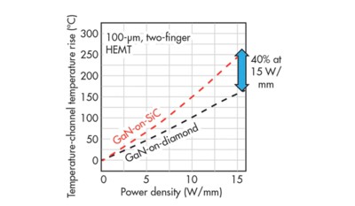
1. A plot of thermal-resistance measurements (peak channel temperature, derived from Raman measurements) demonstrates the heat-transfer superiority of GaN-on-diamond compared to GaN-on-silicon-Carbide. (Source: University of Bristol)
In one example, TriQuint fabricated identical HEMT’s (high electronic mobility transistors) on GaN-on-diamond substrates and GaN-on-SiC substrates. The University of Bristol used micro-Raman methodology to measure thermal resistances of the two transistor types, and found that the thermal resistance of the GaN-on-diamond HEMTs was at least 40% lower than that of the GaN-on-SiC HEMTs1(Fig. 1).

GaN-on-diamond technology offers two key benefits. First, it enables devices that are more than three times smaller than with other approaches, making them less expensive and providing much more power in a smaller form factor.2 Second, devices are able to run in ambient temperatures as much as 50% hotter, thereby lowering the cost of cooling subsystems and ultimately saving on-going energy expense.
High-Voltage Power Devices
High-voltage power devices, such as insulated-gate bipolar transistors (IGBTs), have the advantage of higher efficiency and higher switching frequencies, but generate significant heat that demands extreme thermal-management solutions. For IGBTs, an effective thermal-management solution once again is to bring diamond as close to the heat-generating source in the form of metallized heat spreaders.
High-voltage IGBT applications typically involve switching or converting power for electrical vehicles, train and aerospace power generators, and alternative-energy distribution. In one test case using a 1200-V IGBT, a metallized diamond heat sink replaced a ceramic substrate. It more than halved the junction-to-case thermal resistance, which in turn more than doubled the IGBT’s power rating.
Laser Diode Arrays
High-power laser-diode arrays are found in material processing (e.g., welding and surface treatments), medical applications (e.g., tattoo removal and laser surgery), and applications for pumping high-power solid-state lasers. These arrays require significant thermal management to optimize performance. Adding a diamond heat spreader between the diode array and the submount effectively transports the heat away from small emitter hotspots.
However, the coefficient of thermal expansion (CTE) mismatch between the diamond heat spreader and the laser-diode gallium arsenide (GaAs) can cause reliability issues, as well as the condition known as a “smile”—a slight bend of the horizontal line connecting the emitters. On-going research and development efforts are on ways to effectively solve this CTE-mismatch issue.
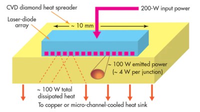
2. A typical synthetic-diamond application would consist of this 200-W laser-diode array mounted on a diamond heat spreader. The same approach could be used for power devices.
Figure 2 shows a 100-W laser-diode array with multiple emitters closely spaced on a single chip. The light output from these emitters is either used directly or collimated with a lens array into a single-beam laser. High power output, wavelength stability, and reliability of these arrays are of utmost importance.

Using metallized heat spreaders to cool laser-diode arrays can significantly increase beam intensity and beam quality, since it allows for closer spacing of the individual emitters in the arrays. In addition, or alternatively, diamond heat spreaders can extend the lifetime of the diode arrays.
Semiconductor Assembly and Test
Certain steps in the test and assembly of packaged semiconductor devices requires that temperature either be kept low enough to prevent device damage, or kept constant across the entire package for optimum assembly quality. Because metallized diamond heat spreaders can transport heat both laterally and vertically at very fast rates, they’re able to rapidly pull heat away from, and spread it evenly across, hot devices.
One example involves cooling of devices during functional test. The device under test needs to operate under a test pattern without a heat sink attached, which may cause it to quickly overheat. Using CVD diamond heat sink effectively addresses this cooling issue without resorting to active water impingement cooling.
In another case, using diamond to rapidly spread heat across a substrate while a flip-chip die is being bonded to it makes it possible to apply the same amount of heat to every solder joint at the same time. This ensures high-quality across an array of 1000 solder joints.
 闽ICP备2021005558号-1
Leave A Message