Pos:
Home KnowledgeTechnologyOptimizing activation process for strong direct bonding between diamond wafer and Si substratesAs semiconductor devices have been continuing to shrink in size and increase in output power, their power density (W/m2) has been rapidly increasing. The power concentration results in hot spots on the devices, which lead to the degradation of device performance, reliability, and product life. In order to solve this problem, it is highly required to develop effective heat dissipation technology from electronic devices.
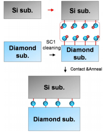
For efficient heat dissipation, device integration techniques onto a diamond heat spreader have been intensively studied. This is because the diamond has the highest thermal conductivity (5 times higher than Cu) among solid materials. For the device/diamond integration, a hydrophilic bonding technique between Si and diamond substrates enables the formation of atomic bonds between the Si and diamond substrates at low temperatures under atmospheric conditions.

While the bonding strength of a diamond (111) surface is over 30 MPa, that of a diamond (100) surface is limited. It is known that the diamond (100) surface has difficulty in the OH termination because of steric hindrance; this is a possible reason for the weak bonding strength by the hydrophilic bonding. However, most of the commercially available monocrystalline diamond substrates have a (100) surface because of their high crystal growth rate. Thus, we have optimized process parameters to form strong bonding of the diamond (100) substrate with the Si substrate.
Firstly, we have demonstrated the bonding experiments with plamsa activation using N2 and O2 gas. When the Si surface was irradiated with RIE using N2 gas, the shear strength was 1.46 MPa. Meanwhile, the shear strength was 1.52 MPa in the case of RIE using O2 gas.
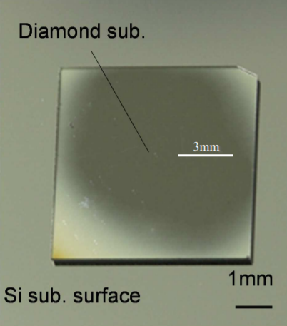
By using the oxygen plasma, the diamond substrate was bonded with the Si substrate. While corners of the diamond substrates were not bonded, around 80% of the diamond was bonded with the Si substrate. As there are no significant differences in the bonding strength, we performed the additional bonding experiments using RIE using O2 gas. Then, we bonded the diamond and Si substrates under different activation times. When the plasma activation time was in the range of 60-180 s, the shear strength was improved with the increase in the irritation time. However, the shear strength decreased by the plasma irradiation longer than 180 s. The highest bonding strength was 1.92 MPa, which satisfied the U.S. military standard.

The diamond (100) substrate, which is the main product in the commercial diamond substrates, was strongly bonded with the Si substrate by the optimized plasma activation process. When the Si substrate was activated by the oxygen plasma for 180 s, the shear strength was 1.92 MPa, which satisfied the military standard. The strong bonding between semiconductor devices on the diamond (100) substrate would facilitate future high-power and high-frequency devices.
 闽ICP备2021005558号-1
Leave A Message