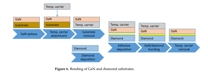
In 2013 BAE Systems proposed a "device-first technology that allowed the placement of the diamond heat spreader within 1 um of the device hot spot . After the complete fabrication of the devices, the wafer was bonded to a temporary carrier and the substrate and the GaN buffer layer were removed. The back side of the HEM Is was then bonded at room temperature (RT) to a 1" square PCD diamond substrate, fabricated in a different step, using an adhesive and pressing the two materials together. Thanks to the low roughness of the GaN back surface after the removal of the buffer layers(<1nm), and depending on the k of the adhesive used, TBRGaN/diamond was estimated to be in the range15-60 m2K/GW. The generic process flow is schematically represented in Figure 6.
In 2014, functional GaN HEMTs originally fabricated in a SiC substrate were bonded to a 1" PCD wafer at a temperature lower than 150°C by means of a 35 nm-thick layer of Si-containing bonding material [110]. The experimental value of TBRGaN/diamond was 34 m2·K/GW and the yield of the bonding process was≈70% (Figure 7a). Even when dissipating 3 times more power, the temperature of the GaN-on-diamond HEMTs was lower than that of their GaN-on-SiC counterparts. However, original GaN-on-SiC devices outperformed GaN-on-diamond ones: ID max and gm peak were reduced by 16% and 11%respectively, after the GaN-on-SiC HEMTs were transferred to diamond. The degradation of the DC characteristics was attributed to changes in residual mechanical stress in the device epitaxial layers during the substrate transfer process, as well as to the mechanical and chemical treatments applied. The RF characteristics of the GaN-on-diamond devices also degraded in comparison with GaN-on-SiC ones: at 10 GHz and for VD = 20 V PAE/PD were 38%/3.4 W/mm and 48%/4.6 W/mm for both devices, respectively, when tuned for maximum power, and 42%/3.0 W/mm and 57%/4.1 W/mm (when tuned for efficiency)According to the authors, this was primarily due to the omission of air-bridge structures in the GaN-on-diamond devices with the unconnected device channels acting as RF parasitics during power measurements.
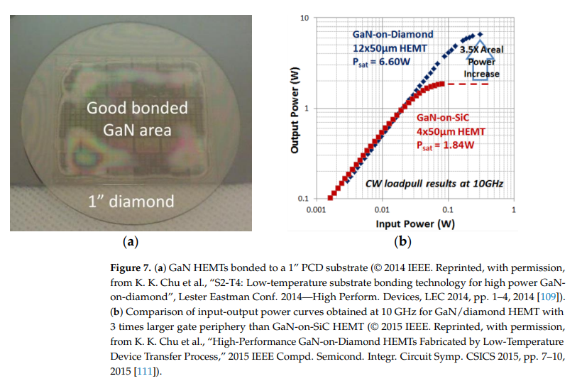
Upon solving these issues, the PAE of 12 x 50 um GaN/diamond HEMTs increased to51% and Pp to 11.0 W/mm at 10 GHz. For the same Vp, the Pp of 4 x 50 um GaN-on-SiCHEMTs was only 9.2 W/mm, showing a 3.5 times areal power increase with GaN-on-diamond HEMTs (Figure 7b). Even under these conditions, the temperature at thecenter gates was slightly lower for the GaN-on-diamond HEMT than for the GaN-on-SiCHEMT (195 against 202 °C, respectively). The main challenge of this process was identified as the ability to achieve large area bonding with very low TBRGaN/diamond.
In 2017, Liu and co-workers bonded HEMT devices previously fabricated on SiC substrates to a 3" commercial PCD wafer at a temperature of 180°C and obtained afunctional device yield over 80%. The experimental TBRGaN/diamond (51 m2.K/GW) was still relatively high and the DC current showed a 12-19% reduction due to self-heating;nevertheless, the peak junction temperature of a 10 x 125 um HEMT with compressed gate pitch of 20 um decreased from 241 to 191 ·C after being transferred from the SiC to the diamond substrate, suggesting a 20% reduction in Rth. CW load-pull measurements were performed at 10 GHz and class A B operation on 4 x 125 m'40 um gate pitk ll!1s,after being transferred to the PCD substrate, the same HEMT delivered 5.5 W/mm Pp with a PAE of 50.5% (against 4.8 W/mm and 50.9% when on the original SiC substrate).
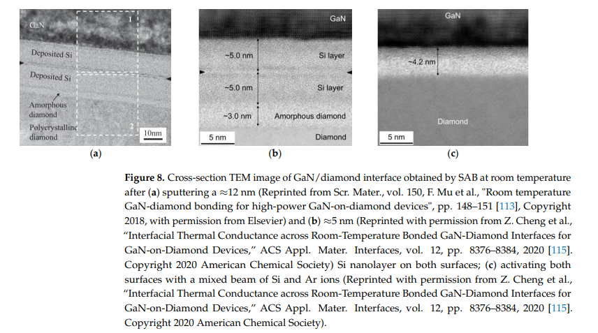
The RT bonding of GaN and PCD films or SCD substrates has also been achieved using surface-activated-bonding (SAB). SAB is a direct solid state covalent bonding method that takes place in ultra-high vacuum conditions without obvious inter facial chemical reactions. The previous bombardment of the to-be-bonded surfaces with an argon (Ar) ion beam induces the surface activation, generating surface dangling bonds and making it possible to bond the surfaces at RT. A few nm-thick Si inter layer is typically sputtered on the diamond and GaN surfaces to improve the adhesion. The two activated surfaces are then pressed together at RT and the dangling bonds form covalent bonds at the interface. Transmission electron microscope (TEM) images of the resulting uniform GaN/diamond interface can be seen in Figure 8a . After the bonding process the Si layer was 24 nm-thick. The bombardment of the diamond surface with Ar ionsinduced its amorphization, creating an additional 3 nm-thick amorphous diamond layer.The thickness of the Si layer was further reduced to 10 nm (Figure 8b), creating an interface with a TBRGaN/diamond of ≈19 m.K/GW. In a slightly different experimental setup, the surfaces activation was performed with a mixed beam of Si and Ar ions; thethickness of both Si interlayer and amorphous diamond layer was reduced to 2 nm Figure 8c) and the TBRGaN/diamond was as low as ~11 m2.K/GW. Despite these interesting preliminary results, functional HEMTs on this GaN/diamond material stack are yet tobe reported.
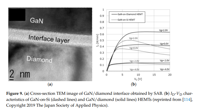
Using a similar SAB method with an intermediate Si nano layer, in 2019 Mitsubishi Electric Corp. announced the successful transfer of a GaN-on-Si multi-cell HEMT to a SCD substrate . No voids were identified in the 6 nm-thick bonding interface and the improved DC characteristics of the GaN-on-diamond devices showed that the GaN HEMTs layers were successfully transferred to the diamond substrate (Figure 9)This achievement is expected to improve the PAE of high-power amplifiers in mobile communication base stations and satellite communications systems, thereby helping tore duce power consumption. Mitsubishi Electric targeted the commercial launch of GaN-on.diamond HEMTS for 2025.
Wang et al. reported bonding GaN and SCD/PCD diamond substrates at RT and in atmospheric air Following the surface activation with Ar ions, a double molybdenum(Mo)/gold (Au) layer (5 nm/11 nm) was sputtered on the surfaces of both materials and they were pressed together with an applied load of 2000 N. The bonded surfaces showeda voidage as low as 1.5% and the bonding strength was evaluated as 6.8 MPa. Even though no thermal measurements were made, after 1000 cycles of thermal cycling between-45 and 125 oC the bonding area remained at 73%, suggesting that the Mo/Au nano layer can effectively balance the difference in the CTEs of GaN and PCD wafers.
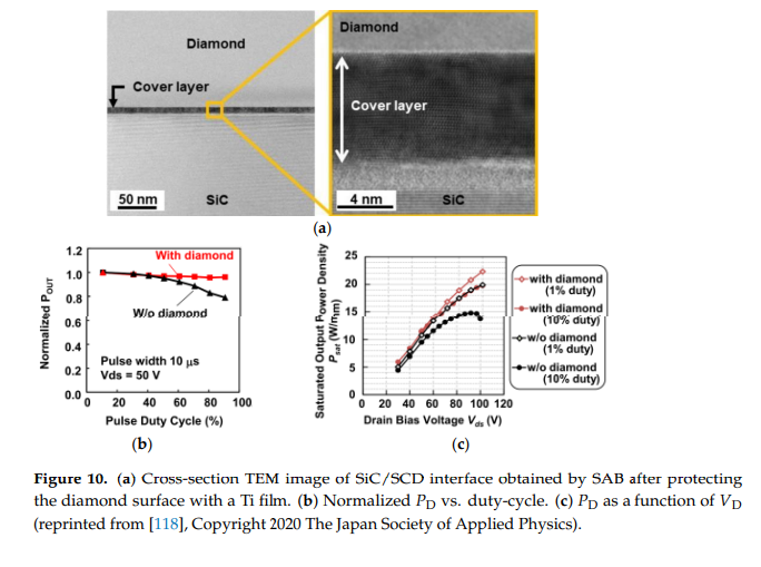
Minoura and his colleagues from Fujitsu Limited bonded AlGaN/GaN and indium aluminum gallium nitride (InAlGaN)/GaN-on-SiC HEMTs to SCD substrates ba modified SAB method. A thin (<10 nm) titanium (Ti) layer was previously deposited on the surface of the SCD substrate to prevent the amorphization of the diamond surface during the bombardment with the Ar ions. The TEM image of the SiC/diamond interface is shown in Figure 10a. Using this method, the TRB at the diamond/SiC interface was66 m2K/GW and the Rh of the AlGaN/GaN HEMT bonded to the SCD substrate was about 1/3 compared to that without diamond. The Pp of In AlGaN/GaN HEMTs measured with pulsed load-pull measurements (for Vp = 50 V a pulse width of 10 us, and 10%duty cycle) increased from 14.8 to 19.8 W/mm with the bonding of the SCD heat spreader structure. With 1% duty cycle, the SCD-bonded HEMT showed a Pp of 22.3 W/mm Figure 10b,c show the variation of the normalized Pp with the duty-cycle and the Pp as afunction of VD, respectively.
SAB of GaN HEMTs and diamond was also achieved by sputtering a 450 nm-thick AlN layer on both GaN AlN nucleation layer (after removal of the Si substrate) and diamond surfaces, followed by surface activation with an Ar*-based plasma and by the rmocompression at 160 °C . The strain relief layers and the AlN nucleation layer prevented the flow of heat from the top GaN layer into the diamond substrate; as a consequence the temperature of the HEMT on the diamond substrate was higher than that on the Sisubstrate.
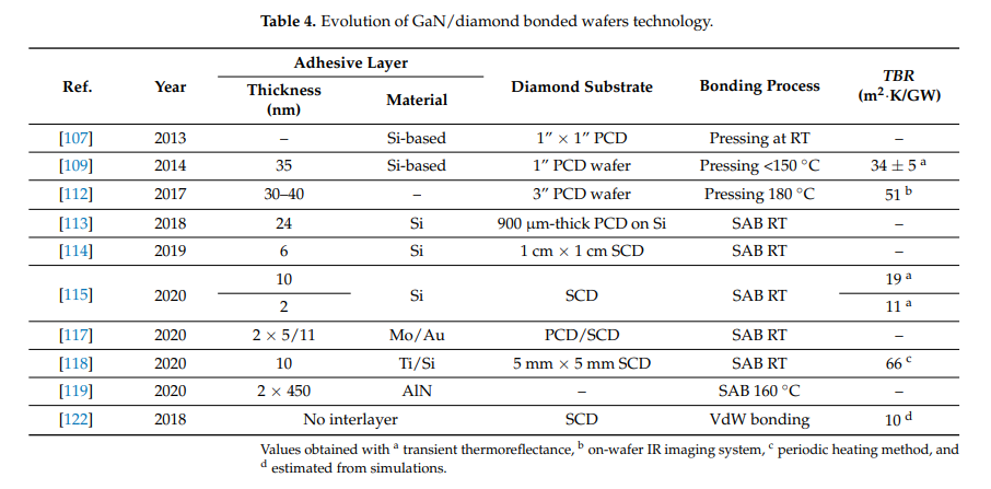
Van der Waals (VdW) bonding, a process first employed for GaAs thin films has also been used to bond GaN devices and SCD/PCD substrates at temperatures below300 °C . This technique guarantees a good thermal interface (TBRGaN/scD wasestimated to be as low as 10 m-.K/GW ) without the observation of stress or degradation. RF-devices operating at 3 GHz with improved efficiency (PAE of 54.2% against 50.6%for GaN-on-Si HEMTs)) were demonstrated with SCD; on the other hand, the bonding obtained with PCD was not reproducible .The evolution of the relevant technological parameters of GaN/diamond bonded wafers is summarized in Table 4. The TBR of the GaN/diamond interface obtained after the SAB and VdW bonding of GaN and SCD can be as low as 11 and 10 m2.K/GW, respectively Functional HEMTs have been fabricated on GaN bonded to SCD and PCD substrates. The electrical parameters of HEMTs fabricated using this method are summarized in Table A2in the Appendix A.
CSMH focuses on the research and production of diamond wafers, and currently has diamond wafer, diamond heat sink , GaN on diamond ,AIN on diamond and other products, providing diamond thermal management solutions for our customers.
 闽ICP备2021005558号-1
Leave A Message