Recently, research teams from City University of Hong Kong, Shanghai University, University of Groningen and Southern University of Science and Technology have made important progress in the field of diamond physical property regulation. For the first time, a large-scale "deep elastic strain engineering" containing two-dimensional helium in diamond lattice confinement was achieved through helium ion implantation at high temperature. The related achievement is titled "Creating Two-dimensional solid helium via diamond lattice confinement". Published in the international journal Nature Communications, the results open up a whole new path for future diamond "fourth-generation semiconductor" applications.
Diamond is expected to become the ideal material for the next generation of microelectronics and optoelectronic devices, and is also known as the "Humumarama peak" of electronic materials due to its excellent properties such as ultra-wide band gap (~5.5eV), low dielectric constant, high carrier mobility, extremely high breakdown strength and corrosion resistance. However, because of the inherent ultra-high hardness and lattice properties, diamond doping is very difficult.
In recent years, a research team led by the City University of Hong Kong has reported for the first time that diamond can achieve an unprecedented super-large bending elastic strain of nearly 9% at the nanoscale, which makes it a revolutionary new strategy to regulate the electronic properties of diamond through "elastic strain engineering". Last year, Professor Yang Lu and his team from the City University of Hong Kong went on to obtain microarray structures from a precision micro-machined monolithic single crystal diamond using in situ nanomechanical methods, and achieved a large uniform global elastic strain of nearly 10% through pure mechanical loading, which can be extended to device arrays. This enables "deep elastic strain engineering" of diamond microelectronic devices, which is expected to be used in the next generation of microelectronics, photonics and quantum information technology. This series of diamond-related work shows that the wide band gap structure of diamond can be regulated and significantly changed to meet the needs of the future development of microelectronics and semiconductors. More importantly, it also inspires more scholars in different fields to explore the controllable adjustment of functional properties of diamond under strain or other extreme conditions.
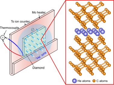
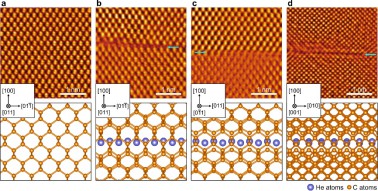
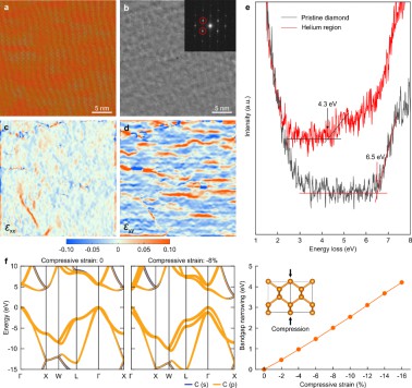
Since helium is insoluble in solids, the injected helium ions will spontaneously precipitate into helium bubbles. By controlling the helium ion implantation process, the team successfully introduced a two-dimensional solid helium disk in a diamond with a 3 mm×2 mm area (see Figure 1) while avoiding diamond amortization and graphitization. The team used iDPC STEM to analyze the crystal structure of a two-dimensional solid helium disk confined by a diamond lattice (see Figure 2). This is the first time that the helium atomic structure has been observed by TEM. The team then found that these high-pressure two-dimensional solid helium disks can exert considerable elastic strains on the diamond lattice (see Figure 3a-d). This unique "strain doping effect" can also significantly alter the electronic properties of diamond, thus obtaining unique applications in future diamond-based semiconductor electronics. Off-axis STEM-EELS measurements showed that the compressive elastic strain caused by two-dimensional solid helium disks narrowed the diamond band gap by up to 2.2 eV (FIG. 3e), a finding that was further confirmed by DFT calculations (FIG. 3f).

FIG. 1 Helium ion implantation in a diamond lattice produces two-dimensional solid helium disks

FIG. 2 iDPC STEM image of two-dimensional solid helium disk

FIG. 3 Strain distribution, energy band measurement and first-principles calculation prediction of strain-doped diamond
The strategy of controlled introduction of material defects paves the way for "deep elastic strain engineering" by introducing and retaining large elastic strains in bulk single crystal diamond. The above ion implantation process can be applied to existing large size electronic grade diamond wafers and other covalently bonded semiconductors with high elastic strength. Further use of mask technology mature in semiconductor manufacturing will effectively control the spatial distribution of two-dimensional solid helium disk to achieve device design and integration in semiconductor planar technology, opening up a new road for future diamond "fourth generation semiconductor" applications.
SCMH is a high-tech enterprise focused on the development and production of third generation (wide gap) semiconductor substrate materials and devices, and is committed to becoming the world's leading wide gap semiconductor materials and devices company. We always uphold the concept of customer first, to provide customers with the best products and services. High quality, high standard of products and services, not only make Huhe electrochemistry has been widely recognized by customers, but also well received in the industry. At present, the company has achieved large-scale production of diamond and aluminum nitride related products. The Diamond wafer Ra<1nm, the thermal conductivity of diamond heat sink 1000-2000W/m.k, and GaN on diamond, Diamond on GaN, diamond-based aluminum nitride products. And has been widely used in 5G base stations, lasers, new energy vehicles, new energy photovoltaic and other fields. In the future, we will continue to improve product quality through manufacturing intelligence, optimize production process and other measures, standard international advanced management level, continue to improve our products and services.
 闽ICP备2021005558号-1
Leave A Message