Pos:
Home KnowledgeTechnologyBoron-Doped Diamond Diode Array with Excellent Rectification and Voltage-Blocking CharacteristicsThrough the thermal diffusion process using heavily doped, bonded SiNM as dopant carrying medium. The process is also simple and easily accessible. We propose that the origin of the successful doping is enhanced boron diffusion into diamond enabled by the Si-C bonding states near the Si–diamond interface, which lower the energy to create diamond vacancies and enhance boron transport.

The graphitization-free process is thought to be directly related to the intimate bonding between Si and diamond. A previous study has shown that introducing impurities at elevated temperature in diamond can prohibit graphitization during thermal annealing.13 In the current thermal diffusion experiment, boron atoms accumulate at the bonded surface of the diamond as soon as thermal diffusion begins to occur at an elevated temperature. Therefore, no phase transition is expected to happen at the SiNM bonded diamond surface under the special thermal diffusion setting. This expectation is consistent with experimental observations.
The above boron doping method is used to fabricate diodes using a 2×2mm2, 120μm thick nSCD plate (Fig. 3). Fig. 3(a) shows the process flow for fabricating vertical p-i junction diodes. After completion of SiNM bonding and boron thermal diffusion from SiNM to diamond (Fig. 1(a-v) the cathode is formed first on the bottom side of the diamond plate. The anode is formed directly on top of the SiNMs (Fig. 1(a-ii)), which previously served as a boron carrying medium, since it is much easier to form ohmic contacts on heavily p-type doped Si. It is noted that a p-i junction is not formed between Si and diamond in this case, but between the p-type doped diamond surface and the intrinsic diamond bulk. Both the anode and the cathode contacts are ohmic contacts. To prove that the p-i junction is formed in diamond not in between Si and diamond, ap-i diamond diode without an SiNM layer, which was removed after completion of boron diffusion, was fabricated. The results are shown in the supplementary material (Fig. S6).43 Fig. 3(b) shows (i) the optical images of the diamond before processing, (ii) the SiNM bonded diamond, (iii) finished diodes, and (iv) the diamond diode array. Fig. 3(c) further shows the scanning electron microscope (SEM) images of the finished diamond diodes. As can be seen here, using the transfer printed and
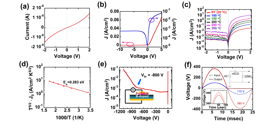
patched SiNMs, selective doping can be easily realized on the diamond surface.Fig. 4(a) shows the current-voltage (I—V) characteristics from two adjacent bottom contacts formed on the diamond surface. The nearly straight I—V curve indicates that accepta- ble ohmic contacts are formed. Fig. 4(b) shows the measured forward and reverse bias (up to —10V) I—V characteristics of the p-i nSCD diode. The diode shows good rectifying behav- ior and the ideality factor is found to be 1.3. The high ideality factor is ascribed to surface conductive channels which are induced during the doping process. The current density in the vertical junction diode is 0.07A/cm2 at þ5V, which is lower in comparison with diamond Schottky diodes.5–8 The low current density is mainly due to the low carrier concentration in the undoped nSCD (see supplementary material for more comparison analysis). Fig. 4(c) shows the measured diode’s I—V characteristics at various temperatures (from room temperature to 300 oC) in order to extract the boron activation energy. As the temperature increased, both for- ward and reverse currents increased, with the forward current increasing faster than the reverse current, leading to an improved rectification ratio and forward ideality factor. The temperature-dependent current behavior is resulted from desirable semiconducting properties of the diamond, similar to the Schottky diodes reported earlier,6 which further indi- cates the potential high temperature application of the diodes. Fig. 4(d) shows the Arrhenius plot of the diodes under zero bias, which is used to obtain the actual activation energy of the boron atoms. Using J0 Ⅸ T5/2 exp(—Ea /kT), where Ea is the activation energy,40 we obtain 0.283eV for Ea, which agrees well with reported values41 under boron concentration reported in this work.
Fig. 4(e) shows the large reverse bias range measurement results of the diodes. The reverse bias
less than one order from 0V to —800V, where diode break- down begins to appear. To our knowledge, this is the highest breakdown voltage that has been reported from a diamond diode. It is also the first p-i diamond diode realized using non in-situ doping methods.3 Considering the shallow boron doping depth that is achieved here, the results indicate the great potential of SCD for power rectification and switching. High quality synthetic diamond has a breakdown electric field of about 107 V/cm. The breakdown electric field of natural diamond is usually about a quarter to half of the value of synthetic diamond. The diamond plate used in this study is 120μm. A simple calculation reveals that the nearly intrinsic bulk diamond is far from being fully depleted before diode breakdown occurs. Since the boron doping depth in the diamond is very shallow and the doping concentration quickly degrades from the top surface (Fig. 2(a)), the boron doped top layer has been fully depleted under certain reverse bias. Hence, further depletion of the bulk diamond is impossible, thus limiting the breakdown voltage of the diodes. It is expected that a higher breakdown voltage would be achieved if the boron doping depth and concentration could be improved (note: 30–60kV breakdown voltage is estimated under full depletion of the 120μm bulk of this nSCD).
The boron-doped single-crystal diamond produced by CSMH can achieve doping from low concentration to high concentration. It has realized a uniform and controllable concentration and a customizable boron doping process.CSMH uses the MPCVD method to prepare large-sized and high-quality diamonds,and currently has mature products such as diamond heat sinks, diamond wafers, diamond windows,diamond hetero junction integrated composite substrates,etc.
 闽ICP备2021005558号-1
Leave A Message