Pos:
Home KnowledgeTechnologyHeat saver! Diamond hot sink sheet makes high voltage power device packaging no longer a difficult problemIn recent years, the manufacturing of power electronic devices is based on the micro-machining and MOS process, which promotes the development of power electronic devices to the direction of integration and modularization. The increasing demand for high voltage and high power and the rapid innovation of process technology promote the development of power devices to the direction of small size, high performance and fast speed. It is the general trend to realize modularization through multi-chip connection during packaging. However, the resulting circuit heat also increases rapidly, which will lead to the rapid accumulation of heat generated per unit volume of power module devices, resulting in the decline of chip life.
The practice shows that the failure rate of the device is 55% because the heat is not lost in time. The life of gallium arsenide or silicon semiconductor chip is greatly affected by the temperature. When the temperature increases by 10℃, the failure caused by the chip is 3~5 times. Because in electronic devices, the working temperature of the circuit is in a state of constant rise, most of the loss is from thermal radiation, if the heat can not be effectively lost, then the thermal expansion coefficient does not match between the material, will produce thermal stress and thermal fatigue, and then lead to the burning power module. Therefore, heat dissipation is a key problem in power electronic devices.

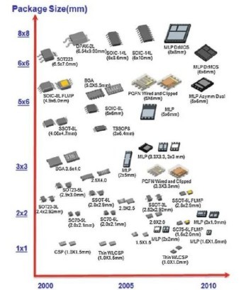
Figure 1. Types and history of power devices
On the one hand, the new generation of Wide Band Gap (WBG) semiconductor materials, such as silicon carbide (SiC) and gallium nitride (GaN), have gradually become a research hotspot because of their better electrical, mechanical and thermal properties than Si. Replacing Si based semiconductors with WBG semiconductors can withstand higher breakdown voltages, achieve faster switching speeds, lower switching losses, and higher operating temperatures. On the other hand, the lack of packaging technology has slowed down the introduction of high voltage wide band gap power modules into the market. Package-related failures account for a large proportion of all failure forms of power modules. Therefore, one of the bottleneck problems to be solved is the failure and reliability of the packaging materials of high voltage power modules under the action of multi-physical field coupling stress.
Generally speaking, electronic packaging includes interlayer medium, frame wiring, sealing materials and packaging substrate and so on several parts, and the packaging system of metal coating, chip and other modules usually have a good heat dissipation ability, so the key to affect the heat dissipation of electronic devices is the insulation substrate material used for packaging. In other words, one of the keys to solve the problem of device heat dissipation is to choose the appropriate packaging substrate.

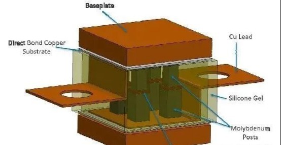
Figure 2. Schematic diagram of the package of power electronic devices
Power electronics packaging substrate is a kind of base electronic component material which is used to carry electronic interconnect and has good electrical insulation performance. It not only plays a supporting and protecting role in electronic circuit and semiconductor chip, but also plays a very important role in heat loss. Power electronic devices often face a complex working environment in the process of use, so the ideal electronic packaging substrate should have the following characteristics:
(1) Higher thermal conductivity, good thermal conductivity is conducive to better heat dissipation;
(2) Low coefficient of thermal expansion, matching that of other materials in the package such as silicon and gallium arsenide;
(3) Good air tightness, resistance to high humidity, high temperature, radiation and corrosion and other harsh environment on the influence of electronic devices;
(4) High stiffness and strength, which can support and protect the circuit and chip effect;
(5) Excellent welding performance and easy processing, can better adapt to various shapes and sizes of the device;
(6) As low material density as possible to reduce the weight of the device.
Common electronic packaging substrates include: organic packaging substrates, metal and metal matrix composites, ceramic - based packaging substrates.
Organic packaging substrate: As a traditional packaging substrate material, organic packaging substrate has low dielectric constant, light material, easy to process into small circuit, suitable for mass production, low cost of manufacturing packaging. However, with the application of more and more high power and large scale electronic devices, the packaging requirements of devices are becoming higher and higher. Due to poor electrical performance, low high temperature resistance, poor thermal conductivity and poor matching with the thermal expansion coefficient of the chip, the organic packaging substrate has been unable to meet the packaging requirements of power electronic devices, especially not suitable for military engineering, smart power grid, aircraft, high-speed rail and other fields of "high air tightness and high pressure and high temperature resistance" product packaging requirements.
Metal and metal matrix composite packaging substrate: insulated metal substrate with its high thermal conductivity, high mechanical strength, excellent electrical conductivity, ductility, good machining performance and other advantages, has been successfully developed and used in electronic packaging. Aluminum matrix composite is a commonly used substrate in metal matrix packaging substrate. It has the advantages of higher specific stiffness and strength, lower density, easy to adjust the coefficient of thermal expansion and so on. It has been widely used in power LED, power electronic equipment, aerospace, hybrid integrated circuit and other industries. Although metal materials have many advantages, they need to be improved in such aspects as abrasion resistance, corrosion resistance, high temperature resistance, high stress on the grain interface and easy to produce cracks, and the production cost of metal substrate is high.
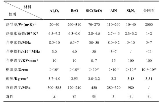
Ceramic based packaging substrate: At present, the commonly used ceramic based packaging substrate mainly includes Al2O3, BeO, SiC, AlN, Si3N4 and so on. However, the thermal expansion coefficient and dielectric constant of Al2O3 are higher than that of Si single crystal, and the thermal conductivity is still not high enough, resulting in that the Al2O3 ceramic substrate is not suitable for use in high-frequency, high-power and ultra-large scale integrated circuits. The thermal conductivity of SiC ceramics is very high, and the higher the purity of SiC crystallization, the greater the thermal conductivity. The biggest disadvantage of SiC is that the dielectric constant is too high, and the dielectric strength is low, which limits its high frequency application, only suitable for low density packaging. AlN material has excellent dielectric properties and stable chemical properties, especially its thermal expansion coefficient is well matched with silicon, which makes it a promising semiconductor packaging substrate material. However, the highest thermal conductivity is only 260W/ (m·K) at present. With the increasing demand for heat dissipation, AlN material also has a certain development bottleneck. Diamond is known to have the highest thermal conductivity in nature. The thermal conductivity of single-crystal diamond is 2200~2600 W/(m.K), and the coefficient of thermal expansion is about 1.1×10⁻⁶/℃. It has excellent properties in semiconductor, optics and other aspects that cannot be reached by other packaging materials.

FIG. 3 Comparison of diamond properties with other packaged substrate materials
As a well-known high-tech company in China focusing on the research and development, production and sales of diamond wide band gap materials, CSMH produces diamond wafer Ra<1nm and CVD Diamond Heat Sink with thermal conductivity of 1000-2000W/m.k. GaN on diamond, Diamond on GaN, diamond-based aluminum nitride and other products are committed to solving the thermal management problems of high-power devices in various industries, and have been recognized by customers in professional fields such as high-speed rail, laser, 5G communication, new energy vehicles, and new energy photovoltaic.
 闽ICP备2021005558号-1
Leave A Message