When it comes to compound semiconductors, few would argue that GaN is one of the key technologies to watch right now. Be it in military sectors, 5G telecom infrastructure or RF front end applications, the high power density and high efficiency material is making in-roads into many industry segments. And having shaken its reputation as an expensive semiconductor for very high-end applications only, rapid market adoption is predicted.
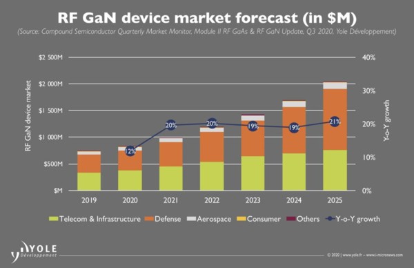
In 2019, yole Développement valued the RF GaN device market at $740 million and forecass this figure to reach beyond $2 billion by 2025. Along the way, GaN-on-SiC will seize market share from industry incumbents, silicon-based LDMOS and GaAs, in Defence, and Telecom and Infrastructure sectors.
Promising market developments are coming from NXP as well as industry partners, US-based II-VI Advanced Materials and Japanese Sumitomo Electric Devices Innovations. Both NXP and the II-VI/Sumitomo duo are building 6-inch GaN-on-SiC facilities in the US, opening the door to that all-important transition from 4- to 6-inch wafer fabrication, and the economies of scale this will bring.
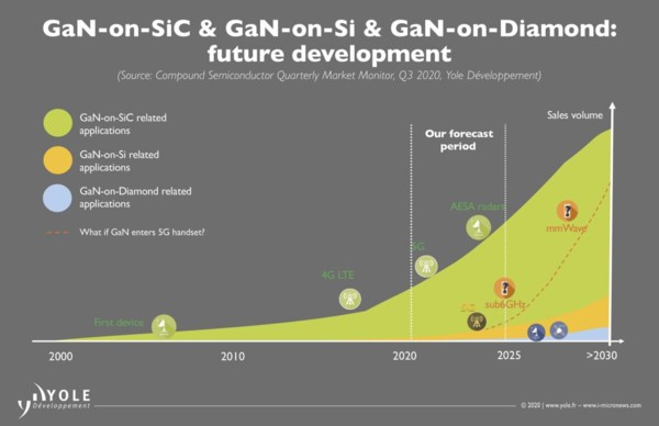
Many eyes are also on less established GaN-on-silicon, which could yet gain a firm foothold in 5G telecom and 5G RF front end applications, thanks to its expandable wafer size, low cost and scalable silicon substrate supply chain. US-based Macom has teamed up with European STMicroelectronics, to develop the technology for telecom OEMs while France-based foundry, OMMIC, also offers GaN-on-silicon processes for mm-wave applications. Other industry players are working on GaN-on-silicon solutions for the exciting 5G handset RFFE applications, but operating in stealth-mode.
Still, nothing can beat GaN-on-Diamond when it comes to performance. Despite eye-watering costs, Diamond offers the highest thermal conductivity of any known material, making this technology ideal for high-end, high power applications including military radar and satellite communications. GaN and Diamond are not easy to bond but companies such as RFHIC, South Korea, and US-based Akash Systems are certainly making headway.
Crucially, the well-publicised US-China trade tensions are having a huge impact on market growth with China, the US and Europe bolstering domestic activities and building a more autonomous RF GaN supply chain to circumvent restrictions. Now the question is when will China become fully-autonomous? Similarly, the political situation has prompted all nations’ supply chains to evolve, setting the scene for a future, strong global market.

A key market for RF GaN has always been defence, with the largest growth, right now, coming from military radar applications including ground-based, airborne, space and ship-borne radar. The move from the old travelling wave tube (TWT) technology to solid-state Active Electronically Scanned Array (AESA) systems has delivered larger detection areas, faster scanning rates, higher spatial resolution and scalability.
These systems now contain thousands of transistors, and thanks to high power density, power-added efficiency and thermal conductivity, GaN-on-SiC can pack high performance into a light-weight, smaller footprint. Given this, the US Department of Defense (DoD) research arm, DARPA, has ploughed more and more cash into GaN for radar applications with industry heavyweights, such as Raytheon, Northrop Grumman and Lockheed Martin, also funding long-term programs.
Europe, Korea and China have followed the US lead, also setting up numerous GaN systems programs. And so GaN-on-SiC transistors and MMICs have progressively replaced LDMOS and GaAs devices.
However, GaN-on-SiC still remains relatively expensive compared to its competitors. Both LDMOS and GaAs transistors are fabricated on 6 inch wafers whilst GaN-on-SiC devices are predominantly produced on four inch wafers. What’s more, compared to silicon, SiC wafer manufacture is in its infancy with the industry’s limited number of SiC suppliers adding to the cost burden.
Still, no other technology looks set to deliver the power density and other advantages of GaN-on-SiC anytime soon, pointing to this being the technology of choice in AESA systems. Factor in growth from other key applications – electronic warfare and military communication – and Yole expects the GaN RF device market for this market segment to reach $1 billion by 2025, representing half of the anticipated market for the GaN RF device sector.

Our existing products and services such as wafer-level diamond/diamond heat sinks/diamond coating can provide professional diamond thermal management solutions for various fields. Welcome to discuss in detail!
 闽ICP备2021005558号-1
Leave A Message