Diamond, hailed as the "ultimate material" due to its ultra-high hardness, wide bandgap, high thermal conductivity, and excellent optical transparency, shows enormous potential in fields such as high-power electronic devices, photonic devices, quantum sensing, and micro-electro-mechanical systems (MEMS).
However, single-crystal diamond films grown by conventional epitaxy are often attached to high-pressure high-temperature (HPHT) diamond substrates. In optical characterizations like Raman, photoluminescence (PL), and cathodoluminescence (CL), substrate signals frequently overlap with those of the epitaxial layer, making it difficult to accurately evaluate the crystal quality and defect state of the epitaxial layer itself. This problem severely restricts the application of high-quality single-crystal diamond films in optical and quantum devices.
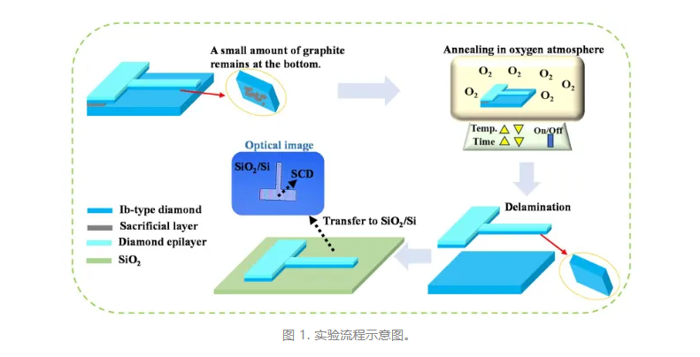
To address this issue, free-standing single-crystal diamond cantilevers and thin plates (SCD MEMS) were fabricated using ion implantation and high-temperature oxygen annealing processes, and then transferred to SiO₂/Si substrates, thereby effectively avoiding substrate interference.

In the experiment, researchers prepared samples through steps including carbon ion implantation, microwave plasma chemical vapor deposition (MPCVD) growth, photolithography, and dry etching. They measured the mechanical resonance characteristics of the cantilevers using a laser Doppler vibrometer, confirming the complete removal of the ion-damaged layer. Subsequently, the samples were systematically characterized using Raman microscopy, photoluminescence, and cathodoluminescence techniques.
The results showed that the full width at half maximum (FWHM) of the Raman spectral peak of the transferred diamond thin plates and cantilevers was only about 1.85 cm⁻¹, which was consistent with the results of the ion-implanted region and much lower than the 1.98 cm⁻¹ of the untreated samples. This indicated that the influence of the substrate had been effectively suppressed. In the PL test, no emission peaks related to nitrogen or other defects were observed, suggesting that the impurity content of the epitaxial layer was extremely low; the nitrogen concentration detected by SIMS was below 10¹⁶ cm⁻³. Further CL testing revealed an exciton emission peak at approximately 236 nm at room temperature, corresponding to an energy gap of about 5.2 eV, which demonstrated that the epitaxial layer possessed high optical purity and excellent crystal quality.
This study indicated that the single-crystal diamond MEMS prepared by "smart peeling" can achieve high-precision optical characterization under the condition of eliminating substrate interference, providing a reliable experimental method for the subsequent design optimization of diamond in optoelectronic and MEMS devices.
The boron-doped single-crystal diamond produced by CSMH can achieve doping from low concentration to high concentration. It has realized a uniform and controllable concentration and a customizable boron doping process.CSMH uses the MPCVD method to prepare large-sized and high-quality diamonds,and currently has mature products such as diamond heat sinks, diamond wafers, diamond windows,diamond hetero junction integrated composite substrates,etc.
 闽ICP备2021005558号-1
Leave A Message