Pos:
Home KnowledgeTechnologyBoron-doped single-crystal diamond, suitable for high-power electronic devicesDiamond has been extensively studied due to its excellent chemical inertness, as well as its resistance to radiation, high temperatures, and pressure. Doping a certain amount of impurities into diamond can significantly improve the lifespan and functionality of many electronic devices. There have been numerous studies on doping during the diamond growth process using the microwave plasma-enhanced chemical vapor deposition (MPCVD) method; doping can alter the properties of diamond, transforming it from a wide-bandgap semiconductor to a metallic conductor and even a superconductor. P-type boron-doped polycrystalline diamond has been applied in devices such as radiation detectors, sensors, and electrodes.

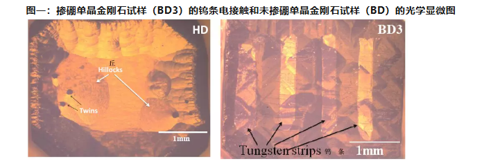
Boron-doped single-crystal diamonds with different concentrations were synthesized homogeneously in the experiment. The seed crystal was pale yellow in color, and the color changed with the incorporation of boron; the color of the boron-doped samples changed from light blue to dark blue. Figure 2 shows the planar AFM image of the epitaxial sample with a scanning area of 20×20μm². The surface morphology of the doped samples was modified after deposition, with seed crystal grinding marks remaining and grooves appearing. Obvious step clustering was observed on the surface of sample BD3.
Figure 3 presents the Raman spectra of boron-doped and undoped single-crystal diamonds. No peaks related to graphitic carbon were observed in the spectra, indicating that the grown homogeneous thin film layers have high quality. There is an intense diamond zone-center phonon mode at 1334 cm⁻¹, and additional broad bands at 580 cm⁻¹, 900 cm⁻¹, 1042 cm⁻¹, and 1233 cm⁻¹. This study also found that the bands around 1233 cm⁻¹ and 580 cm⁻¹ decreased with the increase of boron concentration. In Table 1, the diamond growth rate decreased significantly with the increase of boron content. The diamond growth rate of the undoped sample reached a maximum of 23 μm/h. The high growth rate of sample BD1 may be attributed to the presence of a small amount of nitrogen in the gas and the B/C ratio. For samples BD2 and BD3, despite the same B/C ratio, the lower hydrogen content and lower substrate temperature reduced the diamond growth rate. Overall, the diamond growth rate decreased significantly with the increase of boron content in the plasma.
The resistance of most sample BD3 measured at room temperature was 0.12 Ω·cm. The activation energies of samples BD1, BD2, and BD3 at high temperatures were 0.28 eV, 0.18 eV, and 0.05 eV, respectively; at low temperatures, they were 0.02 eV, 0.05 eV, and 0.03 eV, respectively. The difference in activation energy between high and low temperatures indicates that there are two different conduction mechanisms for carrier transport in the thin film. At high temperatures, carriers are transported through band conduction; at low temperatures, carriers drift in localized states through hopping conduction.
Boron-doped single-crystal diamonds were grown on type Ib diamond seeds with different boron concentrations using the MPCVD method. The boron concentrations of the samples determined by FTIR were consistent with the activation energies obtained by the four-probe tester. The crystal quality was characterized by Raman scattering and X-ray rocking curve. Additional bands were observed in the Raman spectra of the boron-doped diamond films along the first-order Raman peak in the low wavenumber region. A decrease and broadening of the Raman lines were also observed with the increase of boron content in the crystals. Temperature-dependent constant tests showed that the current conduction mechanism depends on the doping content; the samples exhibit semiconductor properties in the temperature range of 90 K-680 K. The conduction mechanism changes from localized hopping to high-temperature band conduction. The minimum resistivity of the sample measured at room temperature is 0.12 Ω·cm, which is suitable for high-power electronic devices.
The boron-doped single-crystal diamond produced by CSMH can achieve doping from low concentration to high concentration. It has realized a uniform and controllable concentration and a customizable boron doping process.CSMH uses the MPCVD method to prepare large-sized and high-quality diamonds,and currently has mature products such as diamond heat sinks, diamond wafers, diamond windows,diamond hetero junction integrated composite substrates,etc.
 闽ICP备2021005558号-1
Leave A Message