Pos:
Home KnowledgeTechnologyAnalysis of Electrical Properties of Boron-Doped Single-Crystal DiamondDiamond possesses a series of excellent electrical, optical, physical, and chemical properties, including a wide band gap, low dielectric constant, low breakdown voltage, excellent thermal conductivity, and high electron-hole mobility. The application of its semiconductor devices holds highly promising prospects in the fields of high-temperature resistance, radiation resistance, and high power. Therefore, the research on the electrical properties of boron-containing diamond is of great significance.
Regarding the energy band of diamond, there exists a large energy gap—known as the band gap—between the valence band and the conduction band. The band gap width of diamond is much larger than that of germanium and silicon. Diamond is a covalent crystal composed of group IV elements, and its physical properties are related to its energy band structure [58]. The energy level diagram of boron-doped diamond is shown in Figure 4.1. After boron doping, the energy band structure of diamond undergoes changes. To detect the variation in its band gap, we employed cathodoluminescence (CL) for research.
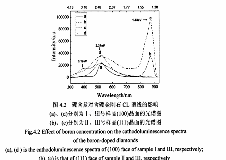
The influence of boron content on the CL spectra of boron-containing diamond is presented in Figure 4.2. Among them, curves a and d represent the spectra of the (100) crystal plane of Samples I and III, respectively; curves b and c represent the spectra of the (111) crystal plane of Samples II and III, respectively. The CL spectral data are listed in Table 4.1. It can be observed that two peaks appear on the (100) crystal plane of diamond, and two peaks also emerge on the (111) crystal plane. By comparing curves a and d, it is found that after boron doping, the intensity of both peaks on the (100) crystal plane of diamond increases, particularly showing a significant enhancement at 3.12 eV, with the ratio of their peak intensities (I/...) reaching 7.89. By comparing curves b and c, it can be seen that the peak at 518 nm in curve b redshifts to 522 nm, and both peaks exhibit a significant intensity increase. This redshift of peak positions and rapid increase in peak intensity are attributed to the increase in boron doping concentration in diamond, which leads to a rise in hole concentration in the crystal, an increase in acceptor energy levels, and consequently an increase in carrier concentration.

Next, by comparing the two peak values in curves b and c respectively, the ratios of the two peaks are calculated as [ratio 1] = 1.503 and [ratio 2] = 2.728, with the latter being much larger than the former. Yasushi et al. studied the cathodoluminescence (CL) spectra of three types of CVD diamond films with different nitrogen doping concentrations. In their research results, as the concentration of donor nitrogen (N) increased, the intensity ratio of the 2.8 eV spectral peak to the 2.3 eV spectral peak in the CL spectra also increased correspondingly. This also indicates that doping in diamond has a significant impact on carrier concentration: an increase in doping concentration leads to a change in carrier concentration, which in turn causes changes in spectral peaks.From the measurement results of CL spectra, it can be observed that as the boron content in the catalyst increases, the intensity of CL spectral peaks enhances. This suggests that the increase in boron content in diamond leads to an increase in carrier concentration, which means the boron concentration in the crystal structure also increases—further enhancing the electrical conductivity of boron-doped diamond.
The CL spectra of [specify the crystal plane, e.g., (110) crystal plane] are shown in Figure 4.4, which differ significantly from the spectra of the (100) crystal plane. Its high-energy peak is located at 2.40 eV, while the low-energy peak is at 1.43 ± 0.01 eV; the former falls within the range of green A-band emission, and the latter within the range of GR1 emission. The latter is defined as a Mössbauer-type emission spectrum, caused by the annihilation of indirect excitons bound to isolated ionized [defects/impurities, context-dependent]. Similar to the (100) crystal plane, the low-energy peak dominates on this crystal plane, and the peak position shifts toward the high-energy direction. The intensities of both peaks increase with the rise in the B/C ratio. It can be seen that after removing the background caused by the tail of the high-energy peak (the broad 2.40 eV band), the intensity of the low-energy emission peak increases faster than that of the high-energy emission peak, with I_C1/I_A1 = 4.71 and I_C2/I_A2 = 13.5. The full widths at half maximum (FWHMs) of the emission peaks at 1.43 ± 0.01 eV in spectra A, B, and C are 0.28 eV, 0.23 eV, and 0.13 eV, respectively. It is evident that as the boron doping amount increases, the FWHM narrows gradually. In addition, the FWHM of the characteristic peak at 2.40 eV is relatively wide.
(1) CL detection of boron-containing single-crystal diamond reveals that the morphology and structure of different crystal planes undergo significant changes. As the boron content in the catalyst increases, the intensity of the cathodoluminescent characteristic peaks of the (100) crystal plane enhances, and new acceptor energy levels appear—with the high-energy peak emerging only after boron doping. This peak can be considered an impurity peak generated by boron doping. For the (111) crystal plane, the intensity of its cathodoluminescent characteristic peaks also increases with the rise in boron content in the catalyst, but the low-energy peak increases faster and exhibits much higher intensity. This confirms that boron atoms are more likely to accumulate on the (111) crystal plane, resulting in a greater increase in the number of holes and a more significant rise in carrier concentration on the (111) crystal plane.
The boron-doped single-crystal diamond produced by CSMH can achieve doping from low concentration to high concentration. It has realized a uniform and controllable concentration and a customizable boron doping process.CSMH uses the MPCVD method to prepare large-sized and high-quality diamonds,and currently has mature products such as diamond heat sinks, diamond wafers, diamond windows,diamond hetero junction integrated composite substrates,etc.
 闽ICP备2021005558号-1
Leave A Message