Pos:
Home KnowledgeTechnologyApplication of Boron-Doped Diamond in Radiovoltaic Effect Isotope Battery DevicesA radiovoltaic effect isotope battery utilizes the built-in electric field of a semiconductor diode to separate the electron-hole pairs excited by radiation in the semiconductor material, thereby generating an electric current and outputting it externally. Therefore, the performance of the semiconductor material has a significant impact on the output characteristics of the device.
As can be seen from Table 1, the band gap width of common semiconductors increases gradually from left to right, with that of diamond being 5.5 eV. As the band gap width increases, the properties of semiconductor materials also change. Due to their large band gap width and radiation-resistant characteristics, wide-band-gap semiconductors are more suitable for applications in extreme environments such as high temperature, high radiation, and high voltage.
Using boron-doped diamond as the substrate, an intrinsic layer with a thickness of 10 μm was epitaxially grown on the diamond surface by the microwave plasma chemical vapor deposition method, and 130 such diamond energy conversion junction devices were fabricated. These devices were then divided into two parts, which were first connected in parallel and then in series. Performance tests were conducted under irradiation with different radioactive sources. The total area of the battery was 1,500 mm². Under irradiation with a Ni-63 source with an activity of 5 mCi/cm², the short-circuit current of the battery was 55 nA. Based on the energy incident into the diamond energy conversion junction, the energy conversion efficiency of the battery reached 5%.

After the battery was irradiated with a Sr-90/Y-90 radioactive source with an activity of 1 Ci/cm² for 1,400 hours, the absorbed dose reached 4,000 rad, while the battery performance remained stable. This should be attributed to the radiation resistance of diamond. It can be concluded that the service life of the diamond isotope battery made with a β-radiation source depends only on the half-life of the isotope used. Subsequently, the battery was irradiated with a Pu-238 α-radiation source, and an open-circuit voltage of 1.85 V and an output power of 36 μW were obtained, with a conversion efficiency of 3.6%. This battery has been used to light up an LED lamp with a current of 15 μA and a voltage of 1.65 V.
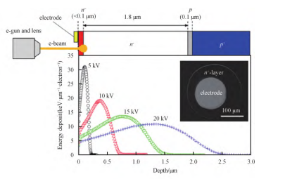
The boron content of the substrate used was ~10¹⁸ cm⁻³, which ensures the crystal quality. However, a high boron content is also crucial for forming a good ohmic contact. Single-crystal diamond with low impurity content and high quality was thinned to 5 μm by means of oxygen/argon ion etching. Subsequently, a highly boron-doped diamond layer (~10²¹ cm⁻³) was epitaxially grown on the diamond film using microwave plasma chemical vapor deposition, and then an aluminum Schottky electrode was fabricated on the back of the diamond film. This device uses the p-type diamond layer as an incident window and the electron beam in a scanning electron microscope as the radiation source, achieving an open-circuit voltage of 1.85 V and a conversion efficiency of 9.4%. This method of epitaxially growing boron-doped diamond on a high-quality intrinsic layer provides a new approach to addressing defects in the epitaxial layer.
Therefore, combining boron-doped single-crystal diamond with β-gallium oxide nanosheets can form a high-performance energy conversion junction device. Type ⅡB diamond with a high boron doping concentration is used as the substrate, and a diamond epitaxial layer with a lower doping concentration is epitaxially grown on the boron-doped diamond via chemical vapor deposition. Then, the surface of the diamond epitaxial layer is modified to reduce dangling bonds after combining with gallium oxide nanosheets, thereby reducing surface states. In this way, an isotope battery device with high energy conversion efficiency can be obtained.
The boron-doped single-crystal diamond produced by CSMH can achieve doping from low concentration to high concentration. It has realized a uniform and controllable concentration and a customizable boron doping process.CSMH uses the MPCVD method to prepare large-sized and high-quality diamonds,and currently has mature products such as diamond heat sinks, diamond wafers, diamond windows,diamond hetero junction integrated composite substrates,etc.
 闽ICP备2021005558号-1
Leave A Message