Pos:
Home KnowledgeTechnologyStudy on Crystal Structure and Properties of Boron-Doped Single-Crystal Diamond Based on XRD and Raman SpectroscopyBoron-doped diamond is a significant material because of its physical and chemical properties such as high hardness superior to cBN, high thermal stability superior to common diamond and chemical inertness to ferrous materials.In addition, the intensity,impact toughness (TI) and thermal impact toughness(TTI) become higher with the crystal size reducing.
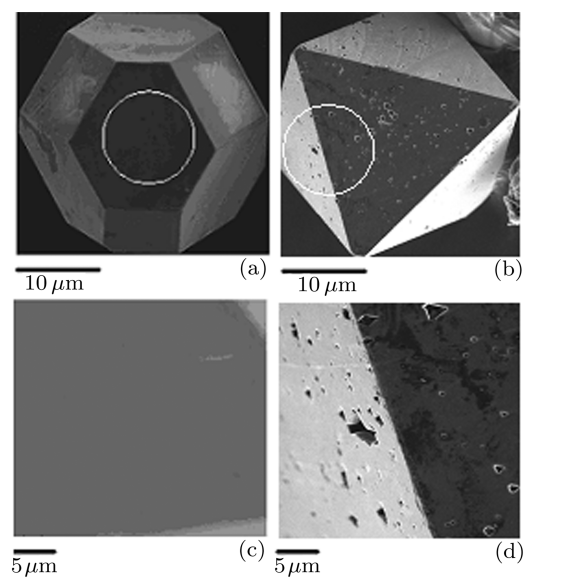
In order to research the crystal structure of borondoped diamond, x-ray diffraction was used to analyse the impurities in diamond crystals. XRD patterns of yellow and black diamond crystals are shown in Fig. 4. From Fig. 4, we can see that only the characteristic peaks of diamond exist in the patterns for both yellow and black diamond crystals. In addition, we find that the {220} peak of boron-doped diamond disappears and its {111} and {311} peaks enhance obviously in Fig. 4(a). This phenomenon is probably related to the change of morphology from cub-octahedral shape to octahedral shape. In other words, boron atoms entered into diamond results in crystal lattice distortion and crystal tropism transforms apparently. The above results show that the boron additive promotes the formation of octahedral diamond, which is consistent with the result of crystal morphology from SEM.

Figure 5 is the first-order Raman spectra of micron grade diamond single crystals at room temperature. Wave number and half peak width of high quality diamond without any adulteration is 1332.5 cm−1 and 3 cm−1 , respectively. The Raman peak and half peak width of yellow diamond is 1332.7 cm−1 and 4.0 cm−1 , respectively, in Fig. 5(a), which is almost consistent with high quality diamond except a little increase of half peak width. While the Raman peak and half peak width of black diamond is 1331.2 cm−1 and 4.9 cm−1 respectively in Fig. 5(b). Contrasted the Raman spectra of diamond with and without additive boron, the excursion of Raman peak toward low wave number and half peak width is −1.5 cm−1 and −0.9 cm−1 , respectively. These results show that boron atoms entered into the lattice of diamond and generally existed on the way of substitution and vacancies, which have influence on lattice structure resulted from the lattice structure stress and defects. The lattice structure stress and defects lead to Raman half peak increasing. This phenomenon is analogous to boron-doped diamond film by CVD,[11] but the mechanism is different.
In a summary, our results show that the V-shape section for micron grade boron-doped diamond growth is variation, the diamond surface is coarse and the x ray diffraction and Raman peaks are changed to different extent due to boron added into the reaction system.
The boron-doped single-crystal diamond produced by CSMH can achieve doping from low concentration to high concentration. It has realized a uniform and controllable concentration and a customizable boron doping process.Lightly B-doped diamonds offer excellent carrier mobility, making them ideal substrates for semiconductor applications. Heavily B-doped diamonds provide low electrical resistance, serving as conductive electrodes for ohmic contacts.Furthermore, it is an ideal material for the fabrication of high-temperature, high-power semiconductor components and can also be used in electrochemistry.Additionally, CSMH offers high-quality diamond wafer substrates (e.g., on Si or SiC), enabling customers to develop advanced semiconductor devices.
 闽ICP备2021005558号-1
Leave A Message