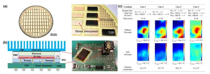
In recent years, with the rapid development of the performance of electronic devices, the effective removal of heat generated by integrated circuit chips (such as CPUs and GPUs) has become increasingly important for ensuring the continuous, stable, and smooth operation of systems. To undertake the fundamental task of heat dissipation and maintain the operating temperature of devices at an ideal level, the development of heat-dissipating materials with high thermal conductivity has become a current research focus.
The thermal conductivity of diamond is more than 10 times that of silicon (Si) materials. Furthermore, compared with gallium nitride (GaN), diamond has higher carrier mobility and a higher breakdown electric field. Therefore, to improve the heat dissipation capacity of semiconductor devices, using diamond sheets or films as heat sinks is widely regarded as one of the promising heat dissipation solutions for the future. Whether it is single-crystal diamond or polycrystalline diamond, their thermal conductivity is much higher than that of other substrate materials, making them a superior alternative to other heat-dissipating substrate materials.

Diamond exhibits ultra-high thermal conductivity. If it can be directly bonded to semiconductors, the high thermal conductivity characteristic of diamond can be fully utilized. The direct bonding method between diamond and semiconductor devices involves first depositing semiconductor materials on a substrate using an epitaxial growth process, then removing the substrate, and performing low-temperature bonding with a diamond substrate. On one hand, this solution avoids the high temperatures required for direct epitaxial growth and reduces high-density dislocations caused by thermal expansion mismatch. On the other hand, this method does not require a hydrogen plasma environment for diamond deposition, thus preventing the degradation of the intrinsic performance of semiconductor devices. In addition, both polycrystalline diamond and single-crystal diamond can be used as heat sink substrates for low-temperature bonding, which greatly reduces the difficulty of preparing diamond substrates. Moreover, since the semiconductor epitaxial layer and the diamond heat sink substrate can be independently fabricated before bonding, the manufacturing process of diamond-based semiconductor devices can be simplified.
Currently, the manufacturing process of diamond-based semiconductor devices enables direct bonding of devices at temperatures below 300 °C, or even at room temperature, significantly improving the heat dissipation capacity of semiconductor devices. In this method, the thickness of the GaN buffer layer is reduced, the nucleation layer is eliminated, and the SiC substrate is replaced with highly thermally conductive diamond through low-temperature bonding technology. This design ensures that the heat source of the GaN device is within 1 μm of the diamond substrate, significantly reducing the device thermal resistance. In this study, a layer of silicon nitride (SiN) was used as the bonding interface layer, and the thermal resistance at the contact interface was as low as 2.5×10⁻⁹ m²·K·W⁻¹. Through continuous-wave direct current (DC) testing, it was found that after the GaN high-electron-mobility transistor (HEMT) was transferred to the diamond substrate, there was no significant degradation in the DC performance of the device. This indicates, to a certain extent, that the stress control during the transfer process and the thermal resistance control at the bonding interface have achieved positive results.
CSMH uses the MPCVD method to prepare large-sized and high-quality diamonds,and currently has mature products such as diamond heat sinks, diamond wafers, diamond windows,diamond hetero junction integrated composite substrates,etc.Among them,the thermal conductivity of diamond heat sinks is 1000-2200w/(m.k), and the surface roughness of diamond wafer a<1nm.It has been applied in aerospace, high-power semiconductor lasers, optical communication, chip heat dissipation, nuclear fusion and other fields.
 闽ICP备2021005558号-1
Leave A Message