As GaN power amplifiers develop toward miniaturization and higher power, their heat dissipation continuously increases, and heat management has become a critical factor restricting the performance improvement of power devices. With an ultra-high thermal conductivity of up to 2,000 W/(m·K), diamond is a highly competitive new heat-dissipating material and can be used as a packaging substrate for high-power devices.
In the packaging structure, the substrate of the GaN power chip is made of SiC material. The chip dimensions are 5.0 mm × 6.65 mm × 0.08 mm, with an active area of 4.28 mm². The chip and the substrate are bonded using Au80Sn20 solder. The substrate has dimensions of 5.0 mm × 10.6 mm × 0.3 mm, and the substrate is connected to the package housing via In80Pb15Ag5 solder. In the simulation model, the solder layer is consistent with the actual tested device, with a thickness of 0.05 mm, and the interface contact coefficient is set based on a 5% void ratio. The computational model uses hexahedral elements for meshing, with a total number of meshes of approximately 300,000.

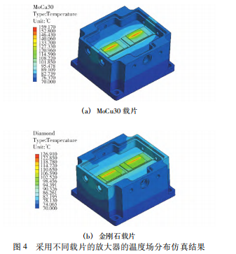
The temperature field distributions of the power amplifiers packaged with the two types of substrate materials were obtained through thermal simulation, as shown in Figure 4. It can be seen from the figure that the junction temperature of the chip with the MoCu30 substrate is 159.17 °C, while that with the diamond substrate is 126.91 °C. Compared with the amplifier packaged with the MoCu30 substrate, the junction temperature of the amplifier with the diamond substrate decreases by 32.26 °C.
Conducting thermal simulation prior to actual production enables the pre-simulation of chip junction temperature distribution and the evaluation and prediction of the temperature of packaged amplifiers. In accordance with the boundary conditions set in Section 2.1, thermal simulation was performed on the power amplifier with a chip heat dissipation of 53 W. Thermal simulations were conducted using five different substrate materials (WCu15, MoCu30, CPC, TU1, and diamond), and the simulation results of the chip junction temperature are presented in Table 3. It can be observed from the table that the comparison of chip junction temperatures among the five substrate materials under the same heat dissipation condition. Except for diamond, the chip junction temperatures of the other four substrate materials are relatively close. Among them, MoCu30 and WCu15 have similar thermal conductivities, resulting in almost no difference in junction temperature. However, WCu15 has a high density and is impenetrable to X-rays, making it impossible to detect the void ratio after sintering; thus, MoCu30 is a better choice. The chip junction temperature corresponding to the CPC substrate is not significantly different from that of the MoCu30 substrate, but the CPC substrate has complex processing technology and high cost. The chip junction temperature corresponding to the TU1 substrate is approximately 12 °C lower than that of the MoCu30 substrate. Nevertheless, the TU1 material is relatively soft, prone to large deformation, and has a significant difference in thermal expansion coefficient from the chip. Compared with the MoCu30 substrate, the diamond substrate with high thermal conductivity reduces the chip junction temperature by more than 30 °C, and its heat dissipation capacity is far superior to that of all other materials.
To further verify the heat dissipation effect of the diamond substrate, thermal simulations were conducted on the power amplifier with a chip heat dissipation ranging from 20 W to 120 W. The relationship between the chip junction temperature and heat dissipation corresponding to different substrate materials was obtained, as shown in Figure 6. It can be intuitively observed from the figure that below the maximum operating temperature of 175 °C for the GaN chip, the WCu15 and MoCu30 materials can only meet the heat dissipation requirement for a heat dissipation of approximately 60 W, the CPC material can satisfy the heat dissipation for a heat dissipation of 65 W, the TU1 material can meet the heat dissipation for a heat dissipation of 70 W, while the diamond can meet the heat dissipation requirement for a heat dissipation of nearly 100 W. Moreover, as the heat dissipation of the power amplifier increases, the gap in junction temperature between diamond and other materials becomes larger, and the heat dissipation effect becomes more significant. Therefore, for high-power devices, the heat dissipation advantage of diamond is particularly prominent.
As a new generation of electronic packaging materials, diamond has received widespread attention and is one of the most promising packaging materials. In this study, a combination of finite element simulation and infrared testing was used to analyze the junction temperatures of power amplifiers packaged with the conventional substrate material MoCu30 and the new substrate material diamond. The results show that the junction temperature of the amplifier packaged with the diamond substrate is reduced by 30.01 °C, approximately 18.69%. Furthermore, finite element simulation was used to compare the heat dissipation effects of diamond with the other four materials under different heat dissipation conditions. The results indicate that diamond exhibits the best heat dissipation effect and can meet the heat dissipation requirement for a heat dissipation of nearly 100 W, which is of great significance for extending the service life of the chip and improving the thermal reliability of power devices.
CSMH uses the MPCVD method to prepare large-sized and high-quality diamonds,and currently has mature products such as diamond heat sinks, diamond wafers, diamond windows,diamond hetero junction integrated composite substrates,etc.Among them,the thermal conductivity of diamond heat sinks is 1000-2200w/(m.k), and the surface roughness of diamond wafer a<1nm.It has been applied in aerospace, high-power semiconductor lasers, optical communication, chip heat dissipation, nuclear fusion and other fields.
 闽ICP备2021005558号-1
Leave A Message