Pos:
Home KnowledgeTechnologyDiamond wafer as the heat spreader for the thermal dissipation of GaN-based electronic devicesBenefitted from the high breakdown voltages (10 times higher than Si), high switching speed (over GHz), compact size, and tunable electronic architecture , III-V nitride semiconductor is becoming one of the best candidates for high-power electronics to enable the increasing power density and high conversion efficiency. The commercialized AlGaN/GaN high electron mobility transistors (HEMTs) have led to the entry into the mediumpower market, and play a central role for the RF and millimeter-wave applications . In the applications of 5G communications, radar, and electronic warfare, the HEMTs devices can offer more than 10 times higher power density than the existing Si technologies .
This giant power induces a huge amount of heat in the chip area, creating localized hot spots with fluxes above 10 kW/cm2 and package-level volumetric heat generation that can exceed 100W/cm−3. The high-level power dissipation results in the challenges using conventional approaches for the thermal management. With the increased power density, self-heating inside the devices becomes an essential issue that accelerates the failure and poor reliability in the real application. Thermal dissipation through conventionally used approaches is no longer adequate. To achieve the effective thermal dissipation, the heat spreader with a much higher thermal conductivity is required. The current GaN wafers are typically grown on sap phie, silicon (Si), silicon carbide (SiC), or free-standing GaN substrates, whose thermal conductivities are 35, 150, 400, and 280W/mK, respectively, which are far from the requirements. The ideal heat spreader would be a substrate that is both highly thermally conductive and electrically insulating. Diamond, with the thermal conductivity up to 2400W/mK at room temperature for the single crystals, and approaching 2000W/ mK for the polycrystals, is the best candidate as a heat spreader for GaN power transistors .
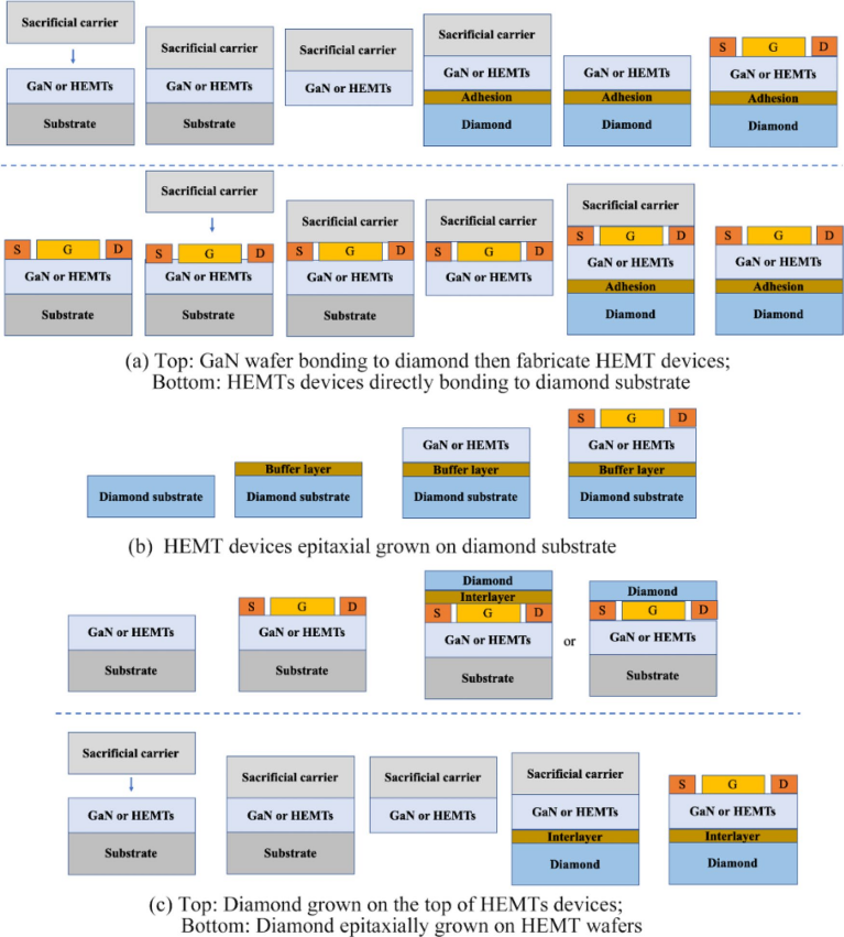
The success of the low-temperature bonding of GaN to diamond enables the device transfer to the diamond technique. The device transfer has the direct advantage of utilizing the standard high yield GaN HEMT process. Chao et al. reported the GaN-on-SiC HEMTs devices transfer to the polycrystalline chemical vapor deposition (CVD) diamond substrate with a maximum drain current density of 1.2A/mm and peak transconductance of 390mS/mm [44]. In this approach, a thin layer of Si-based adhesion was utilized and the bonding process was at the temperature of 150 °C. It was confirmed that the GaN HEMT-on-diamond maintained lower channel temperatures than the original GaN HEMT-on-SiC while delivering 3.6 times higher RF power within the same active area. In 2017, Liu et al. firstly achieved the 3-inch GaN-on-diamond HEMTs device transferred to the diamond substrate at the bonding temperature of 180 °C . The 3-inch device wafer was coated with a thermosetting adhesive layer, then bonded face-down onto a 3-inch SiC temporary carrier wafer. A bonding adhesion layer with a thickness of 15-20nm was deposited onto the exposed GaN as well as on the 3-inch polycrystalline diamond substrate. For a GaN HEMT at the power dissipation of 10W/mm, the peak junction temperature of the device was decreased from 241 °C to191 °C after transferring to the diamond substrate. A maximum current density of ∼1A/mm and a power density of 5.5W/mm CW at 10GHz with the power added efficiency (PAE) of 50.5% were achieved . By using a finite-element analysis, the TBReff of 19m2 K/GW was obtained in the GaN-on-SiC device, while the TBReff in the GaN-on-diamond was estimated to be 51m2 K/GW.

CSMH uses the MPCVD method to prepare large-sized and high-quality diamonds,and currently has mature products such as diamond heat sinks, diamond wafers, diamond windows,diamond hetero junction integrated composite substrates,etc.Among them,the thermal conductivity of diamond heat sinks is 1000-2200w/(m.k), and the surface roughness of diamond wafer a<1nm.It has been applied in aerospace, high-power semiconductor lasers, optical communication, chip heat dissipation, nuclear fusion and other fields.
 闽ICP备2021005558号-1
Leave A Message