Despite the major innovations in lower-power processes and more-efficient designs, getting heat away from semiconductor devices is still a major challenge. Among the reasons for this is that the expectations placed on systems inevitably seem to grow back to fill the available thermal capacity.
While the industry has made enhanced cooling a priority, the entire thermal situation is constrained by the laws of physics, and it’s difficult to turn those to advantage. The thermal path is usually well defined, typically going, for ICs and discrete devices, from die to package to PC board or top-side heat sink, possibly to chassis rails, to cooling air flow (active or passive) or perhaps fluid coolant and finally, to the “outside” (passive devices such as resistors have similar problems). Sometimes that outside is thermally friendly, often it is not.
Often, the greatest impediment in obtaining thermal relief is the tiny distance from the device die to the package. There are some well-known techniques for reducing this barrier, but the thermal resistance of that tiny spot is still relatively high. For this reason, there has been a significant amount of materials-science research devoted to the problem. After all, if you can’t do that effectively, the virtues of the rest of the heat-removal path will be wasted and made irrelevant
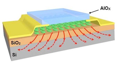
Two examples show the extent of the work underway. The first, led by a team at the University of Illinois at Chicago College of Engineering, is based on an experimental transistor with silicon oxide for the base, carbide for an ultrathin two-dimensional layer, and aluminum oxide for encapsulating material (Figure 1 ).

Figure 1 A University of Illinois team has developed an experimental transistor in a unique layered approach which provides superior thermal characteristics. (Source : University of Illinois)
The objective was to improve the thermal transport at the interface of 2D materials with their 3D substrates, and the researchers claim they have achieved some success, detailed in their paper “Enhanced Thermal Boundary Conductance in Few-Layer Ti3C2 MXene with Encapsulation” and its supplementary material. They reported that at room temperature, the thermal boundary conductance (TBC) of their design increased from 10.8 to 19.5 MW m−2 K−1 upon AlOx encapsulation (note that thermal conduction is not the inverse of thermal impedance; get a clear explanation here).
While this research effort is just that at this point – there’s a much-more dramatic-sounding path being pursued by some organizations, some of it with DARPA support. They are using diamonds to reduce the thermal barrier between die and the outside world. No, these are not gemstones that they are attaching to a die or junction, although that would get some real attention. Instead, they are doing things such as depositing diamond heat sink layer to create a synthetic diamond interface layer.
Why diamond? It is not because of its perceived value as a gemstone, or its use in many industrial applications due to its hardness. It is that diamond has extremely high thermal conductivity of 895 W/m-K, far better than heat-conducting metals such as aluminum (237), silver (429), and copper (401); see “Why does diamond conduct heat better than graphite?“. In addition, it’s also an excellent electrical insulation with electrical resistivity of natural diamonds on the order of 1011 to 1018 Ω-m (the value depends on internal impurities, which also affect its color).
The use of diamond layers for improved thermal conductivity is not just a laboratory R&D project. A recent cover feature in Microwave Journal , “Diamonds are a High-Power Engineer’s Best Friend,” provided distinct perspectives from five vendors who are actively pursuing this approach and even offering off-the-shelf solutions. Each offered a unique perspective on the substrate, process, and products related to diamond-film thermal advances.
Note that diamond thermal benefits are not limited solely to active devices. The story’s segment from Smiths Interconnect showed an 0402-size RF resistor that can dissipate 20 W (continuous)/200 W (pulsed), manufactured using a chemical vapor disposition (CVD) process (Figure 3 ). If you have ever struggled with the tradeoff of physical sizing of an RF power-sensing resister versus its maximum dissipation, you’ll know that this is an impressive rating for that size.
Any advances in easing the heat path from a die, substrate, or junction out to the “away” flow would be welcome, of course. Perhaps an unforeseen and unintended consequence of using diamonds in active and passive devices would be the wider, mass attention such work might receive and even attract some more students to the arcane world of materials science and associated physics.
Have you ever encountered a diamond-layered component in either an experimental or production design? Do you see diamond heat sink as a viable long-term thermal interface that will ease the cooling challenge.
 闽ICP备2021005558号-1
Leave A Message