Pos:
Home KnowledgeTechnologyApplication of Diamond wafer in Thermal Management of GaN High Power DevicesAs a third-generation semiconductor material, GaN has higher spontaneous polarization coefficient and larger piezoelectric coefficient, which can withstand higher power density and is suitable for high-frequency, high-temperature, and high-power electronic devices. However, with the development of power devices towards miniaturization and high power, the thermal accumulation effect in the active region of the chip has prevented GaN devices from fully utilizing their high power performance advantages. When the temperature of the device rises, the device characteristics such as leakage source current, gain, output power, and lifespan may deteriorate or even fail. Research has shown that for every 10-12 ℃ increase in junction temperature, the lifespan and reliability of devices will decrease by 50%. Heat dissipation has become one of the main bottlenecks limiting the development of GaN power devices. To solve this problem, various heat dissipation methods have been proposed to reduce device temperature. Among them, the research and development of new electronic packaging materials has become the technical key to solving the heat dissipation problem of GaN power devices.
Diamond has a thermal conductivity of up to 2000W/(m·K), and is currently known to have the highest thermal conductivity among natural materials. Therefore, diamond has gradually become the preferred packaging material for GaN devices. In recent years, diamond has made significant progress in both technology and application as a heat sink material and substrate material for GaN devices.
Researchers used diamond as a transition heat sink for high-power semiconductor lasers and tested the output characteristics of the laser. The results showed that diamond as a packaging material has excellent heat dissipation performance. The test results provide a reference for using diamond as a heat sink for packaging high-power devices.
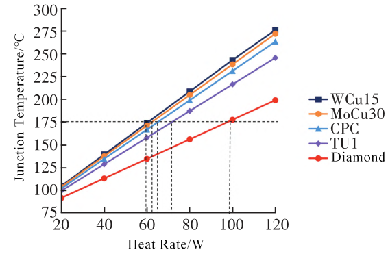
The experiment used different carrier materials to package a GaN power amplifier with a heat consumption of 53W. Finite element simulation and infrared thermal imaging were used to simulate and test the chip junction temperature of the amplifier. The results showed that the junction temperature of the amplifier packaged on diamond chips was reduced by 30.01 ℃, about 18.69%, compared to the amplifier packaged on molybdenum copper (MoCu30) chips. Further comparison with other commonly used carrier materials shows that under the same working conditions, the amplifier packaged with diamond carrier has the lowest junction temperature, and as the heat consumption increases, the heat dissipation ability of diamond becomes more prominent. Diamond can meet the heat dissipation requirements of GaN power amplifier with a heat consumption of 100 W at a safe operating temperature below 175 ℃.

Diamond, as a new generation of electronic packaging materials, is one of the most promising packaging materials. CSMH is committed to the production, research and sales of diamond materials, mastering the latest thermal management solutions for high-power semiconductor devices. It has mature products such as diamond wafers, diamond heat sinks, diamond windows, diamond heterointegrated composite substrates, etc. Among them, the thermal conductivity of diamond heat sinks is 1000-2200W/(m.k), which can fully meet the requirements of high-power semiconductor device substrates or heat sinks.
 闽ICP备2021005558号-1
Leave A Message