Pos:
Home KnowledgeTechnologyHigh Power GaN-on-Diamond HEMTs Fabricated by Low-Temperature Device Transfer ProcessSize, weight and power (SWaP) constraints significantly exacerbate the thermal management problem in military systems. The need to design smaller electronic packages with more powerful components fitting into ever tighter spaces makes thermal management that much more important and challenging. Since heat adversely affects both performance and reliability of electronics, good thermal management through reductions in bulk and interface thermal resistances in electronic components is of utmost importance.

In most modern military electronic systems, the electronic devices often are the heat sources in the system. In many cases, thermal resistance of high-power electronic components can be as large as that of the remaining elements of the system combined. Moreover, heat spreaders, heatsinks or coldplates are often separated by multiple physical layers and interfaces from the device active region where heat is generated and therefore cannot materially affect the device junction temperature. Since the junction temperature of a power transistor is limited by its intra-chip heat spreading capability, one needs to place materials with high thermal conductivities immediately adjacent to the hot spot of the chip to minimize device temperature rise.
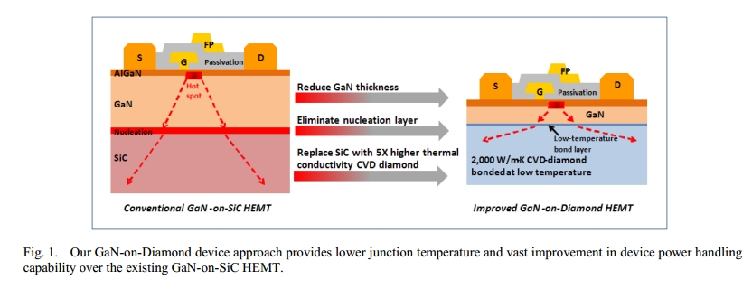
Finite-element thermal modeling is performed for GaN device chips in typical RF module housing configuration. Assuming 3X higher gate packing density and thus 3X higher power dissipation on diamond, the GaN-on-Diamond devices are able to achieve similar or lower junction temperature compared to industrystandard GaN-on-SiC devices when the GaN/diamond bond interface possesses a thermal boundary resistance of approximately 35m2K/GW. This TBR requirement is further relaxed at higher baseplate temperatures. Our modeling results indicate superior power handling capability can be realized with our low-temperature device transfer GaN-on-Diamond process. This technology will in turn enable higher power RF sources in smaller footprints, and major reductions in system SWaP due to associated relaxation of prime power and cooling requirements.
CSMH has been committed to the research and development and production of diamond materials. Now it has products such as diamond heat sink sheet,diamond wafer, diamond window to provide customers with a comprehensive thermal management solution.
 闽ICP备2021005558号-1
Leave A Message