Compared with routine silicon based and scintillation detectors, the electronic grade chemical vapor deposited (CVD) diamond detectors show a lot of advantages attributing to the unique properties of diamond, such as low permittivity (5.7), wide band-gap (5.5eV), high breakdown voltage (107V/cm), high heat conductivity (20w/cm⋅K), high carrier mobility and radiation hardness.More importantly, the high quality of electronic grade SCD diamonds give further advantage for fabricating detectors, e.g. priming is not apparent and largely unnecessary, and polarization effects can be avoided. Detectors based on these diamonds are also stable under the extreme environment of strong magnetic fields, high voltages or high temperatures. Therefore, diamond detectors have been widely applied in tokamak fusion experiments for the diagnostic of thermal neutrons and fast ions.
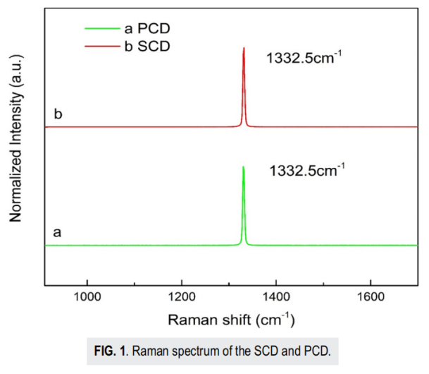
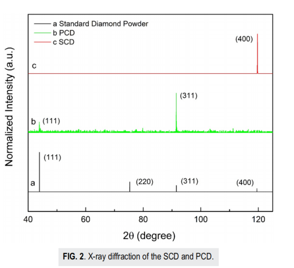
The Raman spectra and X-ray diffraction measurements of the two diamond films are illustrated in Fig. 1 and Fig. 2 respectively. The Raman spectra were obtained using a Raman spectroscope (Renishaw inVia) with 532nm excitation wavelength, and scanned from 900cm-1 to 1700cm-1. From Fig. 1 we can see that the Raman spectra exhibit a strong sp3 bonding peak at 1332.5cm-1 without any sp2 (G and D bands) non-diamond peaks between 1500cm-1 and 1600cm-1 or any other peaks anywhere in the measurement range. The measured full width at half-maximum (FWHM) of the two samples are 4.1cm-1 and 4.5cm-1, which are roughly the limit of the spectroscope, indicating the good quality of the two films.
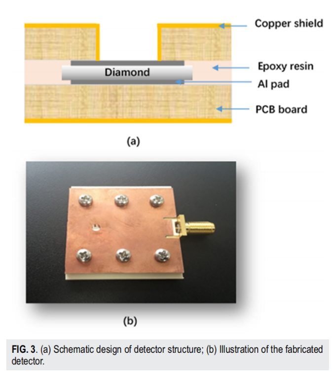
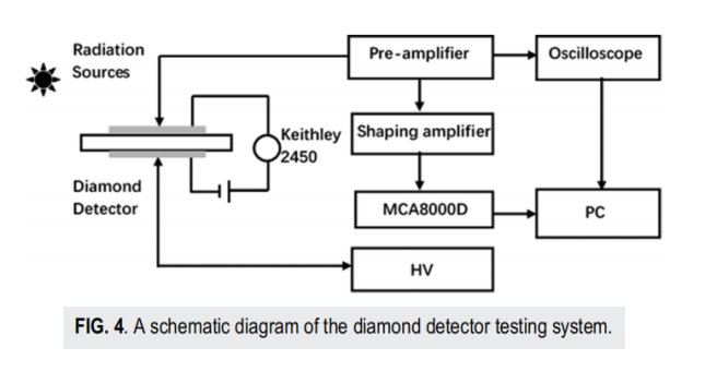
Two particle detectors were designed and fabricated using above SCD and PCD films. Fig. 3 demonstrates the detailed design structure of the devices. The fabricated detector was tested using the characterization system shown in Fig. 4.
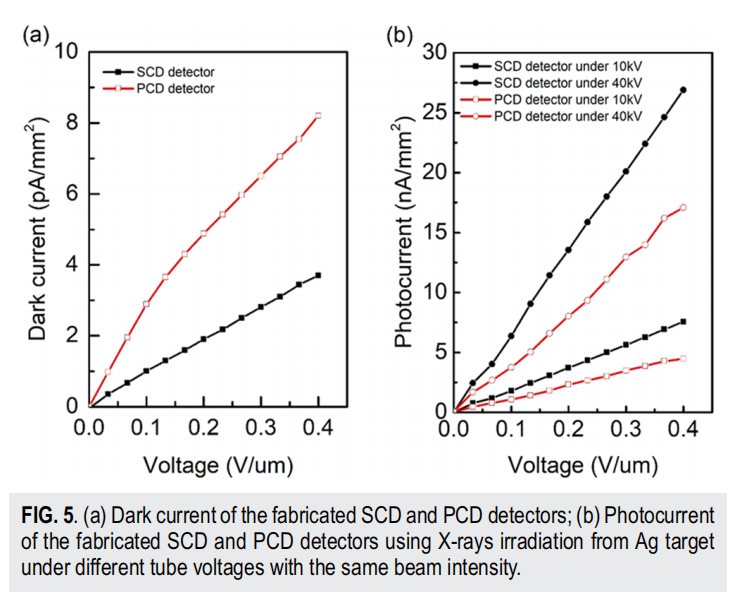
Dark current and photocurrent are important ways to characterize the electrical properties of the radiation detector. Fig. 5(a) and (b) show the dark current (Id) density and photocurrent (Ip) density per unit area of the electrode pad of the two diamond detectors we fabricated via their IV curves. The photocurrent was measured under X-ray radiation produced from an Ag target with a tube operated at 10kV and 40kV acceleration voltage with equal currents. It is seen that the dark current is linear with the applied field for the fabricated SCD detector but the PCD detector is nonlinear over the whole voltage range measured and becomes approximately linear for the larger applied fields. The absolute value of the dark current for the SCD is about 9.2 [pA/mm2 ]/[V/µm] and that of the PCD is about 20.5 [pA/mm2 ]/[V/µm]. The dark current of the SCD is mainly due to the presence of impurities or defects, while that of the PCD is also due to the grain boundaries. Comparing to other reported values, both these values are one or two orders smaller and show the superb quality of the diamond film we used.
CSMH is a high-tech enterprise focusing on the research and development, production and sales of wide band-gap semiconductor materials and is committed to becoming the world's leading wide band-gap semiconductor materials company. The existing core products are diamond wafer (Ra < 1nm), CVD diamond heat sink (thermal conductivity up to 1000-2200W/m.k), diamond window,diamond and GaN heterointegration,AIN on diamond,etc.,which can be used in the production of detector.
 闽ICP备2021005558号-1
Leave A Message