Pos:
Home KnowledgeTechnologyLow Temperature Bonding Diamond Wafer to Si by Using Au Thin-layer for High-power Semiconductor DevicesAs the semiconductor devices are getting higher frequency, higher power and smaller size, the management of thermal dissipation becomes a big challenge. Thermal accumulation increases rapidly in the active region of electronic devices, forming local hotspots and leading to the significant degradation of performance. The application of diamond as heat dissipation substrate for high-power semiconductor devices has been placed great expectation due to its ultra-high thermal conductivity. In this study, Au thin layer was used for the low temperature bonding of diamond and Si.

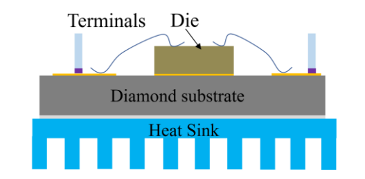
Figure1 Schematic diagram of a diamond based high-power semiconductor device
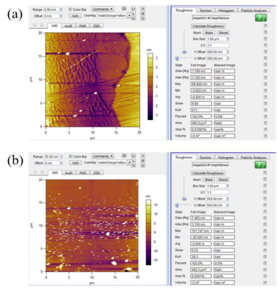
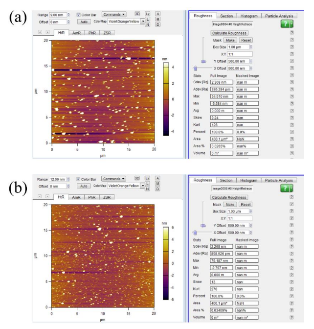
The CVD deposited diamond films were 0.7 mm in thickness and were cut into plates with size of 10mm×10mm. The diamond plates had being ground and polished. Then they were carefully cleaned. Physical vapor deposition (PVD) method was used to deposit 5nm Ti/200nm Cu/5nm Ti/20nm Au on diamond plates. At the same time, Si plates (10mm×10mm×0.6mm) were cleaned and deposited with 5nm Ti/20nm Au. Diamond-Si pairs were alignment together and pressed by hand. They could be pre-bonded at room temperature. Then they were bonded in a vacuum chamber with 200℃ and 6MPa. As control experiments, Si-Si pairs were bonded with the same parameters. Scanning acoustic microscope (SAM) was used to determine the bonding porosity. Atomic force microscope (AFM) was used to characterize the surface roughness.

Figure2 AFM results of diamond surface: (a) after clearning, (b) after PVD.

Figure3 AFM results of Si surface: (a) after cleaning; (b) after PVD.
In this study, Au thin layer was used for the low temperature bonding of diamond and Si. The Au-Au atomic diffusion bonding was successfully achieved. Clean processes were optimized.
CSMH focuses on the research and production of diamond wafers. At present, it has diamond wafers, diamond heat sinks, GaN on diamond, AlN on diamond and other products. In the fields of laser diodes, power transistors, and electronic packaging materials, it can provide customers with diamond solutions.
 闽ICP备2021005558号-1
Leave A Message