Pos:
Home KnowledgeTechnologyApplication of three-dimensional diamond wafer / graphene hybrid array in thermal interface materials“Overheating” is a major problem in the modern electronics industry because of miniaturized and lightened gradually, which can seriously affect the service life and normal operation of the devices [Citation1–3]. It is well known that micro gaps are filled with air, which is seriously affected heat dissipation. Thermal interface materials (TIMs), such as phase change materials and thermal pads, hold a dominant position for rapid heat transfer in microelectronics and microsystems [Citation4–7]. Numerous studies have shown that diamond and graphene composites, by other methods such as annealing, vapour deposition, laser melting and high temperature, and high pressure [Citation8–10], exhibit good mechanical properties and high electrical conductivity, show great application potential as TIMs in the natural world [Citation11].
Traditional carbon-based TIMs are made by filling diamond particles, graphene nanosheets, and carbon nanotube (CNT) array into an organic polymer matrix [Citation12–14], and also methods of injecting polymers into diamond foam skeletons, graphene networks, vertical arrays of structured graphene paper, and CNT [Citation15–18]. On comparison, carbon-based TIMs with a vertical alignment of 3 D materials, instead of random orientation, are highly desirable to break through the performance bottleneck of current TIMs. To obtain vertically aligned architecture of TIMs, researchers have done many works, including, graphene paper lateral stacking [Citation18], constructed by in situ growth [Citation19], electric field-assisted [Citation20], and chloroform-assisted methanol-based plasma enhancement [Citation21,Citation22], etc. However, it is still difficult to achieve batch production due to the complexity and the less practicality.
Here, using a unique one-step microwave plasma chemical vapor deposition, n-butylamine, as the liquid source to prepare a novel high thermal conductivity 3 D vertical diamond/graphene (VDG) hybrid arrays films. The orientated 3 D thermal conduction path of the VDG is regulated by the growth temperature, and the through-plane thermal conductivity value of the VDG700 films up to 97 W m−1 K−1. In the actual TIM performance measurement, the system cooling efficiency with our VDG as TIM is higher than the state-of-the-art commercial TIM, demonstrating the superior ability to solve the inter-facial heat transfer issues in electronic systems.
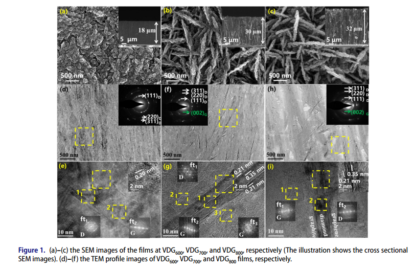
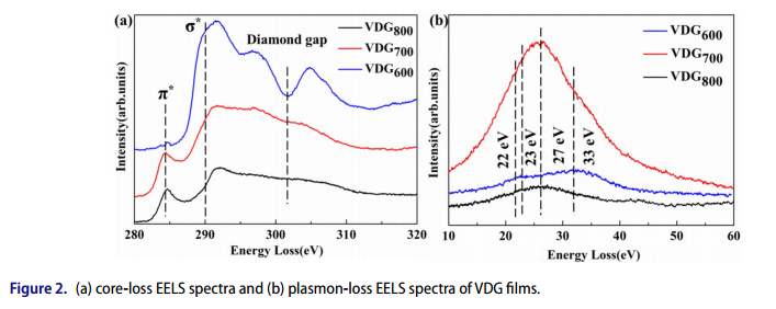
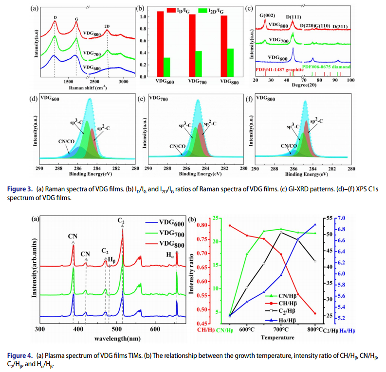
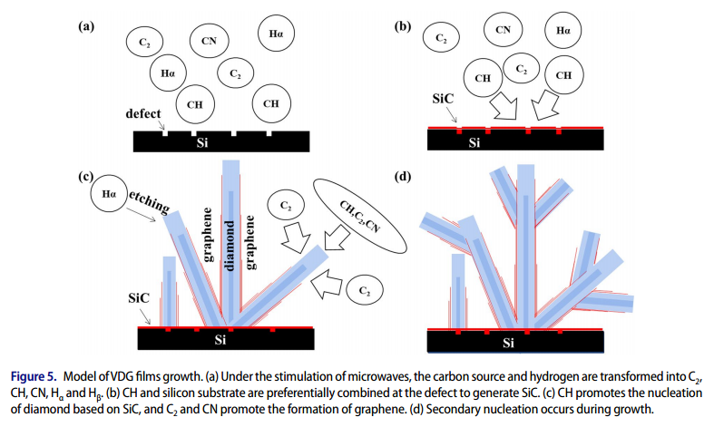
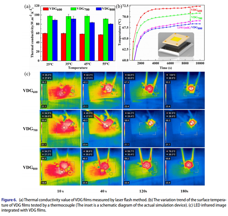
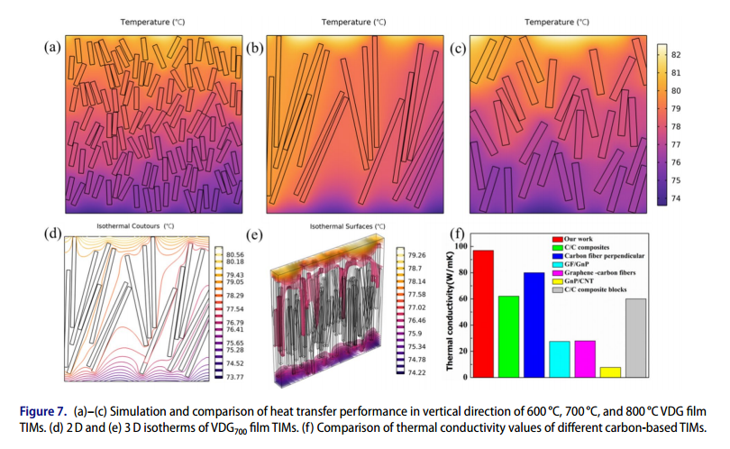
In summary, the VDG films with 3 D thermal conductive networks were successfully prepared using the one-step MPCVD method. Combined with the thermal simulation results and the characteristics of diamond and graphene, it is found that the VDG film TIMs has good thermal conductivity in the transverse and longitudinal direction, which demonstrates that, the VDG film with the “core-shell” structure has a continuous thermal conductivity path, featured with great heat dissipation which is conducive to heat dissipation. The VDG700 film had the highest through-plane thermal conductivity value (97 W m−1 K−1) among the three samples, and the VDG800 film is lower than the silicone pad with the best thermal conductivity on the market according to practical thermal simulation. From the element simulation methods analysis, the VDG700 film indeed has the highest thermal conductivity value in the longitudinal direction. This study provides a simple and practical way of constructing vertically aligned architecture and efficiently improves thermal conductivity for the TIMs application.
CSMH focuses on the research and production of diamond wafers. At present, it has diamond wafers, diamond heat sinks, GaN on diamond, AlN on diamond and other products. Among them, high-power semiconductor lasers packaged by diamond heat sinks have been used in optical communications. In the fields of laser diodes, power transistors, and electronic packaging materials, it can provide customers with diamond thermal management solutions.
 闽ICP备2021005558号-1
Leave A Message