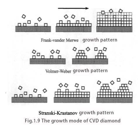
In the initial nucleation stage, according to the lattice mismatch and surface and interface energy, the film can be divided into three different growth modes : Frank-vander Merwe mode ; volmer-Weber model ; stranski-Krastanov model 14648 ]. Fig.1.9 shows the three growth modes of CVD diamond.
( a ) Frank-vander Merwe ( layered growth ) mode : many two-dimensional crystal nuclei are formed on the bottom and grow up to form a single atomic layer. After covering the substrate, the above process continues, and the growth is carried out in a layered growth mode, that is, the whole film is deposited layer by layer, and finally a continuous film with a certain thickness is formed.
( b ) Volmer-Weber ( island growth mode : many three-dimensional island nuclei are formed on the substrate and grow to form a polycrystalline film with rough surface. The surface film has high roughness and a large number of defects inside the structure.
( c ) Stranski-Krastanov ( intermediate growth ) mode : If the grown film material has a large lattice mismatch with the substrate material, the strain energy gradually increases with the increase of the deposited atomic layer due to the different lattice constants. In order to relax this part of the energy, when the film grows to a certain thickness, the growth mode is transformed into an island mode. This mode usually occurs in the case of stress in the film after the growth of the layered mode.

For CVD diamond, due to the high surface free energy of diamond, the growth of Frank-vander Merwe mode on many substrate materials is limited. Generally, only diamond prepared by homogeneous epitaxy can grow in Frank-vander Merwe mode. In general, CVD diamond films prepared by heteroepitaxy are grown in Volmer-Weber mode, and finally grow into polycrystalline films with rough surface. According to different growth conditions, the crystallization properties and quality of diamond films are also very different.
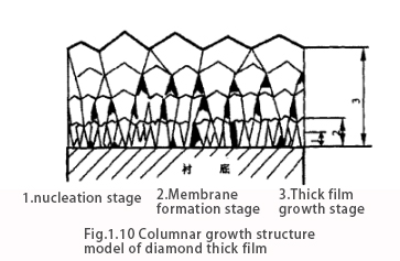
The growth process of CVD diamond thick film is mainly divided into three stages, namely nucleation, formation of continuous film and thick film growth. Figure 1.10 gives the columnar growth structure model of diamond thick film.
In the nucleation stage, nucleation density is an important factor affecting the microstructure of thick films. Therefore, in order to promote the nucleation rate of diamond film, higher methane concentration is generally used.

In the film formation stage, the crystal nucleus grows to form small grains, and the adjacent small grains grow together during the growth process, and the combined growth results in a continuous polycrystalline film.
In the thick film growth stage, the lateral growth of the merged grains is restricted by the adjacent grains and can only grow along the longitudinal direction, forming columnar grains.
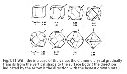
The crystal growth morphology is the external reflection of its internal structure, and the relative growth rate between the crystal planes determines its growth morphology. The ( 100 ) and ( 111 ) crystal planes are the two main crystal planes for diamond growth. The growth rate ratio of ( 100 ) and ( 111 ) crystal planes is defined as the growth coefficient α :
A = 31 / 2V ( 100 ) / V ( 111 )
V ( 100 ) and V ( 111 ) are the growth rates of ( 100 ) and ( 111 ) planes, respectively. For natural diamond or high temperature and high pressure diamond, when α = 1, the grains are cubic ; when α = 2.85, the grains are octahedral ; when 1 < α < 2.85, the grain is cubic octahedron ( see Figure 1.11 ).

CSMH focuses on the research and production of diamond wafers. At present, it has diamond wafers, diamond heat sinks, GaN on diamond, AlN on diamond and other products. Among them, high-power semiconductor lasers packaged by diamond heat sinks have been used in optical communications. In the fields of laser diodes, power transistors, and electronic packaging materials, it can provide customers with diamond thermal management solutions.
 闽ICP备2021005558号-1
Leave A Message