The technique to fabricate GaN-on-diamond wafers involves the epitaxial deposition of GaN on the diamond substrate. However, the deposition of epitaxial GaN films on SCD on PCD substrates is inherently difficult, however, due to a series of factors .First, the large lattice mismatch between the two materials (around 13%) can generate defects and lead to poor crystal quality. lt should be mentioned, however, that the lattice mismatch between GaN and sapphire is even higher (16%), so this fact alone is not determinant. In addition to the lattice mismatch, the large difference in the CTEs of diamond and GaN (0.8 x 10⁻⁶K-1 against 5.6 x 10⁻⁶K-1, respectively, whereas the CTE of sapphire is 7.5 x 10⁻⁶K-1) can lead to a highly stressed interface that will further impact the dislocating density and lead to the possible cracking of the GaN layer. Finally, in the case of PCD substrates, the absence of a fixed epitaxial relationship between the GaN and the diamond increases the difficulty of nucleating a continuous epitaxial GaN layer.
Nevertheless, different groups have tried to grow GaN on diamond substrates. First reports date from 2003, when Hageman and co-workers reported the growth of 2.5 μm-thick polycrystalline and hexagonal GaN films on natural SCD by a dual step A thin GaN layer was initially grown by MOCVD on a 10 nm-thick AIN nucleation layer previously deposited on the SCD substrate. Subsequently, the MOCVD pre-grown sampleswere used as templates for the growth of thick GaN layers using HVPE. The group later reported the growth of 0.07-1.55 μm-thick GaN films on (001) SCD HPHT substrates by MOCVD.
Using a different method, Dussaigne et al. reported the growth of 1 μm-thick GaN epilayers on 100 nm-thick AlN layers previously deposited on HPHT SCD substrates by ammonia (NH)-source MBE. The films displayed a low RMS roughness of 1.3 nm and some cracks due to the difference in the CTEs of diamond and GaN; cracks were not formed for GaN epilayers with thicknesses lower than 250 nm. In a subsequent work, 200 nm-thick AIN and GaN strain engineered inter layers were deposited on topof the AlN buffer layer. An 800 nm-thick GaN layer with 8 x 10 cm-2 dislocation density was then grown, followed by 24 nm of AlGaN (with an Al content of 28%). A 2DEG formed at the interface, allowing the fabrication of HEMT structures with ID max= 730 mA/mm,ɡm peak= 137.5 mS/mm, and ƒT/ƒmax= 21/42.5 GHz.
Following a different approach, researchers from NTT Corporation reported the formation of a 2DEG in an AlGaN/GaN heterostructure formed on a 600 nm-thick GaNlayer epitaxially grown on a type Ib (111) SCD substrate by metalorganic vapor-phaseepitaxy (MOVPE) with similar dislocation density (8.4 x 109cm-2). The AIN/GaN stress-relief layers were deposited on a 180 nm-thick single crystal AlN buffer layer deposited on the diamond substrate and the fabricated AlGaN/GaN HEMTs showed ID max= 220 mA/mm and ƒT / ƒmax = 3/7 GHz. The Rth of GaN-on-diamond HEMTs was 4.1 K· mm/W, against 7.9 Kmm/W for similar GaN-on-SiC structures. By depositing the GaN layer on type lla (111) SCD diamond substrates, Rth was further decreased to 1.5 K-mm/W and RF operation with 2.13 W/mm output power density and 46% PAE was achieved . The impact of the misorientation angle of the (111) SCD surface on the surface morphology of the HEMT structures was also studied by the authors .
Other groups reported growth of GaN on PCD and NCD substrates. The benefits of this approach would be twofold: large-area PCD substrates are available from a few vendors,and the price/area is significantly lower than the one of HPHT SCD substrates. However,only polycrystalline GaN films could be initially deposited. Van Dreumel et al. deposited polycrystalline GaN layers by MOCVD on the surface of nanocrystalline diamond(NCD) films previously deposited by HFCVD on Si substrates, while Zhang et al. deposited fine grained polycrystalline GaN films by MOCVD on the nucleation surfaces of freestanding PCD films prepared by glow discharge. The final goal in this last work was the fabrication of diamond/GaN surface acoustic wave devices, though, and not the fabrication of AIGa/GaN HEMTs.
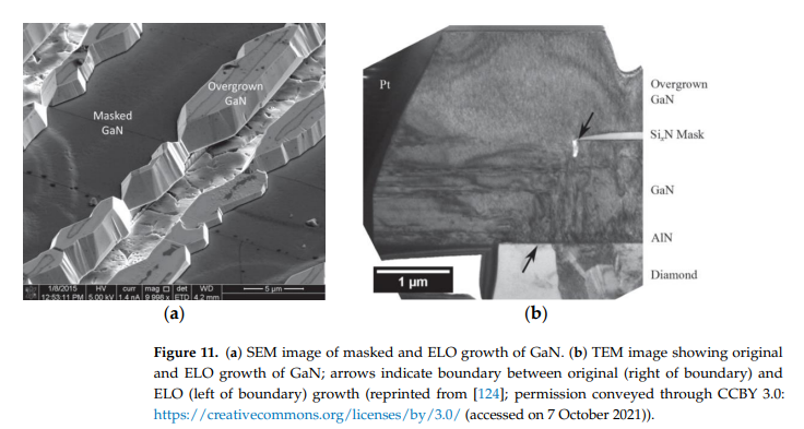
More recently, Webster et al. reported the ability to grow epitaxially-oriented GaN films on thick PCD substrates by MOVPE. An AlN layer was previously deposited at 650 °C as nucleation layer for the subsequent growth of a 1.5 μm-thick GaN layer at higher temperature, on top of which the AlGaN/GaN HEMTs structures were fabricated SiN stripes were then deposited on the AlGaN/GaN stack and the unmasked regions wereetched down to the PCD substrate. After an epitaxial layer overgrowth (ELO) re-growth cycle the dislocation density of the GaN layer was reduced by two orders of magnitude from≈7 x 10⁻⁹ to<108 cm-2). With this technique the team was able to grow GaN with a significant degree of epitaxial orientation on an area up to 15 μm' on a PCD substrate Figure 11. The appearance of some cracks on the GaN surface was attributed to the large difference between CTEs of diamond and GaN.

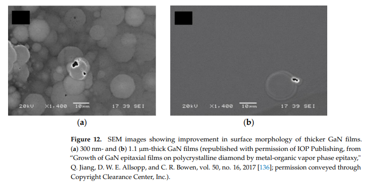
Later the team proposed a different approach; the (111) Si substrate from commercial diamond-on-Si substrates was etched, exposing the back surface of the PCD substrate that was shown to feature a thin SixC layer formed during the deposition of the PCD on the Si substrate. According to the authors, this SixC layer provides sufficient crystallographic information for the epitaxial growth process to occur. Following the etching of the Si substrate, the PCD films exhibited some curvature, due to the thermal stress caused by the high diamond deposition temperatures and the difference in the CTEs of both materials. AlN or Al0.75Ga0.25N nucleation layers were grown on the SiC layer and GaN was deposited by MOVPE. Interestingly, the growth on the nucleation surface of the curved diamond substrate was shown to effectively remove the surface defects induced by the non-single crystalline nature of the SiC layer and to reduce the tensile stress induced by the CTE mismatch, allowing the growth of crack-free GaN epitaxial layers up to 1.1 μm thick. As the thickness of the GaN layers increased, the dislocation density was significantly reduced(Figure 12). Upon optimization of the whole process, the tensile strain inherent in GaN epitaxial layers grown on PCD can be further reduced, and thicker crack-free GaN layers can be deposited. Since the increase of the thickness of the GaN epitaxial layer is usually accompanied by reductions in the dislocation density, the use of thicker GaN layers is expected to have a positive impact on the performance of HEMT devices fabricated using PCD substrates.
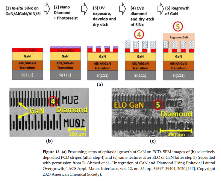
In 2020 Ahmed et al. also proposed the use of ELO to integrate GaN and PCD diamond; the processing steps are represented in Figure 13. Unlike the procedure described in], where the GaN was deposited directly on the PCD by MOVPE, the AlGaN/GaN stack capped with a thin SiN layer was initially deposited on a Si substrate by MOCVD500 nm-thick stripes of PCD were then selectively deposited on the SiN by HFCVD following the procedure described in ; the exposed SiN was then removed by reactiveion etching (RIE) and the GaN surface was made accessible (step 4 in Figure 13a). The wafer was then returned to the MOCVD reactor for the ELO of GaN (step 5 in Figure 13a)Figure 13b,c show the SEM images of the final structure before and after the regrowth step respectively. A continuous GaN film formed across 5 μm-wide diamond stripes separated by 5 um-wide GaN windows oriented along the (1100) direction of the initial GaN. The dislocation density on ELO GaN (≈107cm-2) was≈ 2 orders of magnitude lower than on initial GaN (≈109cm-2). Although coalescence was achieved, several voids, pinholes and cracks were visible in some locations along the coalescence regions; the cracks were generated due to the release of thermal stress energy upon cooling of the wafer following GaN growth. In order to obtain the final GaN/PCD final devices, some steps are further required: MOCVD growth of the HEMT structure, removal of Si substrate and exposure of diamond strip.es surface, thick diamond CVD, and transistor fabrication.


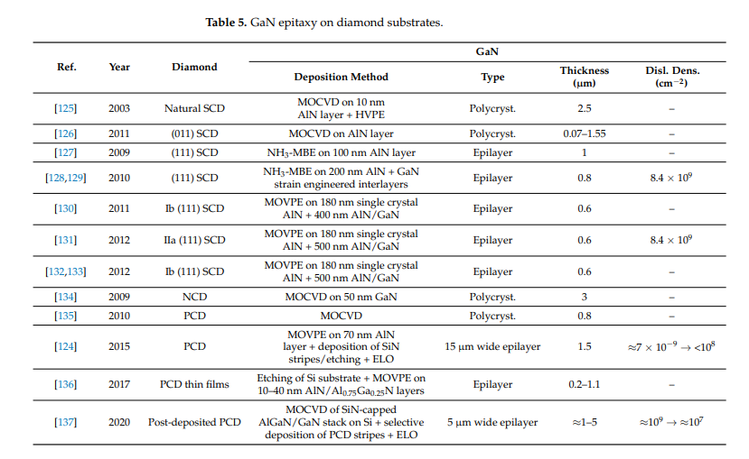
The experimental results obtained so far are compiled in Table 5. As a summary one can say that research efforts focused on both SCD and PCD substrates, however functional HEMTs have only been fabricated on SCD substrates. Despite promising results, the interest on these substrates faded away and more recent research focused on the ELO of GaN films on PCD substrates with reduced dislocation density. The electrical parameters of HEMTs fabricated on GaN films deposited on SCD substrates are summarized in Table A3 in the Appendix A.

CSMH has made breakthroughs in the three combination schemes of GaN & Diamond. The existing diamond heat sinks for GaN on Diamond, Diamond on GaN and GaN & Diamond bonding are world-class. The technical indexes of electro-deposited diamond heat sink and wafer-level diamond products have reached the world 's leading level. The surface roughness of wafer-level diamond growth surface is Ra < 1nm, and the thermal conductivity of diamond heat sink is 1000-2200W / m.K.
 闽ICP备2021005558号-1
Leave A Message