Pos:
Home KnowledgeTechnologyElectric pump laser key!Efficient heat dissipation perovskite lasers using a high-thermal-conductivity diamond substrateHigh efficiency cooling scheme with low temperature rise is one of the key factors to realize electric pumped laser. High thermal conductivity diamond is expected to overcome the heat dissipation limitation of perovskite laser. In this paper, the team demonstrated a diamond-based perovskite nanosheet laser that can efficiently dissipate heat generated during optical pumping. In addition, a tight optical binding is achieved by introducing a thin SiO2 spacer layer between the nanosheet and the diamond substrate. The quality factor of the laser is as high as ~1962, and the laser threshold is 52.19 μJ/cm2. The sensitivity of diamond substrate to pump energy densivity is low (~0.56± 0.01K /μJ/cm2) due to its high heat dissipation.
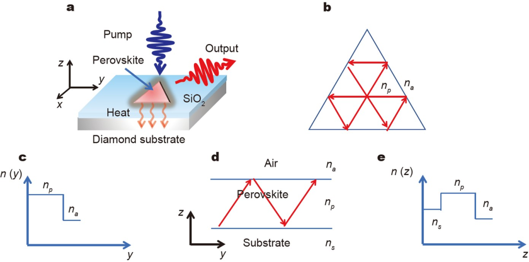
Figure 1 (a) Schematic of a perovskite nanoplatelet laser on a diamond substrate with a SiO2 gap layer. (b) TIR wave propagation paths inside a triangularperovskite WGM cavity in the transverse plane. (c) Refractive index profile in the transverse plane of the nanoplatelet. (d) TIR wave propagation paths in thevertical direction inside the triangular perovskite nanoplatelet cavity. (e) Refractive index profile in the vertical direction of the nanoplatelet that can provide TIR.
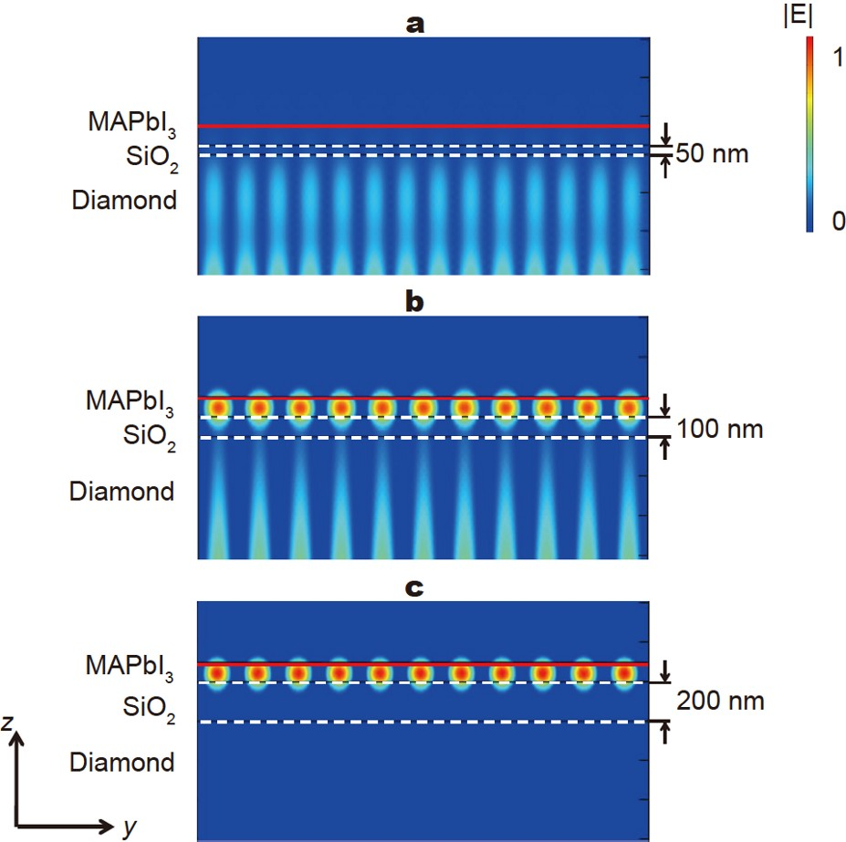
Figure 2 Electric field distributions of MAPbI3 nanoplatelet on diamond substrates with different thicknesses of SiO2 gap layers: (a) 50 nm, (b) 100 nm, and (c) 200 nm.
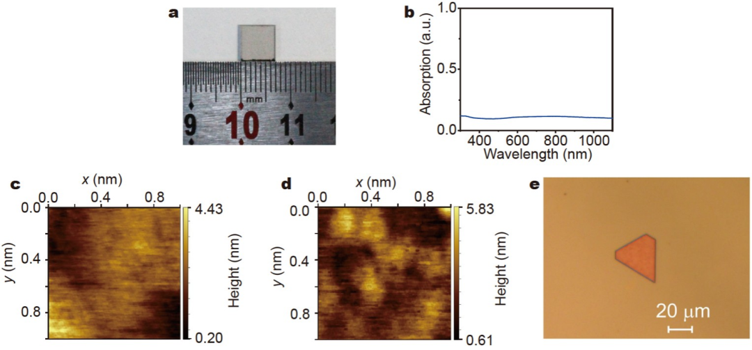
Figure 3 (a) Image of a diamond substrate. (b) Absorption spectrum of the diamond substrate. AFM images of (c) the diamond substrate and (d) SiO2 gap layer. (e) Microscopy image of a perovskite nanoplatelet transferred on the diamond substrate.

Figure 4 (a) 2D pseudo-color plots of emission spectra as a function of P for a perovskite nanoplatelet laser on a diamond substrate with a 100-nm-thick SiO2 gap layer. (b) Integrated emission intensity of the nanoplatelet laser as a function of P. (c) FWHM of the emission peak of the laser as a function of P.
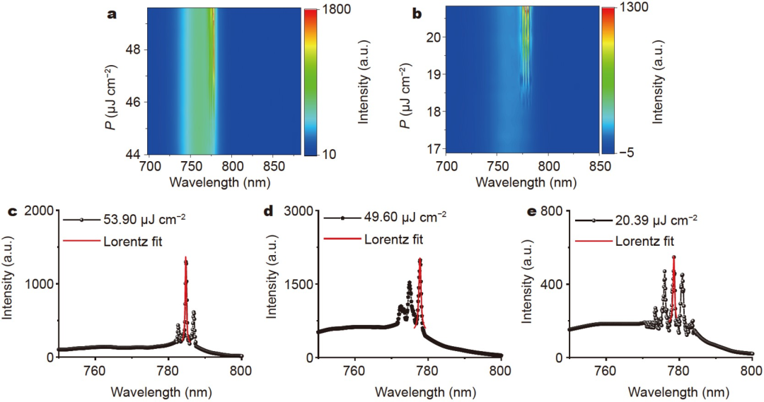
Figure 5 2D pseudo-color plots of emission spectra as a function of P for a perovskite nanoplatelet laser on (a) a diamond substrate with a 200-nm-thick SiO2 gap layer and (b) a mica substrate, respectively. Emission spectra above the threshold with Lorentz fitting for perovskite nanoplatelet lasers on diamond substrates with (c) a 100-nm-thick SiO2 gap layer, (d) 200-nm-thick SiO2 gap layer, and (e) mica substrate, respectively.
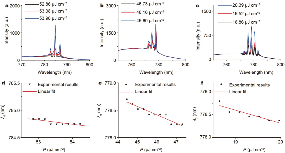
Figure 6 Emission spectra at different pump densities above the threshold for nanoplatelet lasers on (a) a diamond substrate with a 100-nm-thick SiO2 gap layer, (b) a diamond substrate with a 200-nm-thick SiO2 gap layer, and (c) a mica substrate. λ0 as a function of P for nanoplatelet lasers on (d) a diamond substrate with a 100-nm-thick SiO2 gap layer, (e) a diamond substrate with a 200-nm-thick SiO2 gap layer, and (f) a mica substrate.
文章信息
 闽ICP备2021005558号-1
Leave A Message