Pos:
Home KnowledgeTechnologyHow to reduce the "self-heating effect" of GaN devices? Diamond wafer show their talents!The theoretical output power density of GaN power devices can reach more than 40 W/mm, but due to its own thermal effect at this stage, the power density of GaN HEMT devices is only 3~5 W/mm, which shows that its own advantages are far from being exerted. . The main reason is that in the working state of high bias voltage, the excessive power dissipation causes the device to heat up, while the traditional low thermal conductivity substrates and heat dissipation pathways have limited heat dissipation capacity, which hinders the diffusion of heat to the surrounding environment, thereby enhancing phonon scattering. , causing the carrier mobility in the potential well to decrease and the static I-V characteristics of the device to decay, a phenomenon known as the "self-heating effect".

Heat dissipation path of traditional AIGaN/GaNHEMT Device Mean Time Between Failure vs. Temperature
The comparison results of common substrate materials and common properties of GaN are as follows. Relying only on traditional substrate materials (silicon, silicon carbide) and passive cooling technology, it is difficult to meet the heat dissipation requirements under high power conditions, which seriously limits the potential of GaN-based power devices. freed. Therefore, to improve the reliability of the device, it is necessary to solve the problem of heat accumulation in the active area, and to improve the internal heat transfer capacity, especially the heat transfer capacity near the active area, has become a key way to improve the power density of the device and achieve high power characteristics. Using diamond with high thermal conductivity as the heat dissipation substrate or heat sink of GaN-based power devices is expected to improve its "self-heating effect" and realize high-frequency and high-power applications.

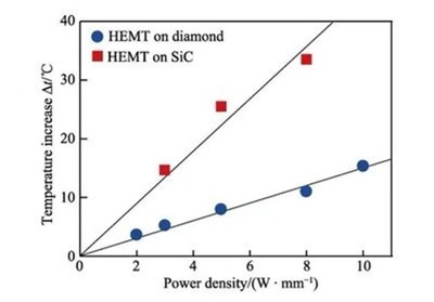
Studies have shown that compared with traditional GaN-based power devices on SiC, GaN-on-diamond devices have higher heat dissipation capabilities, and for the same power density, GaNHEMTs on diamond can reduce the channel temperature at least lower than that of GaNHEMTs on SiC 40%, which will increase the device life by about 10 times, and is expected to realize the miniaturization and high power of GaN-based power devices, thereby promoting a wide range of applications in RF power devices and microwave power devices.

Comparison of temperature rise of AIGaN/GaN HEMT on diamond and SiC substrates.
In the research of diamond-gallium nitride bonding, the bonding of diamond and gallium nitride is one of the main technical lines. However, in wafer bonding, high requirements are placed on diamond quality. For successful bonding, the diamond surface roughness value Ra must be less than 1 nm, ideally less than half of this value, that is, Ra < 0.5 nm. CMS uses the MPCVD method to prepare high-quality diamond heat sinks, and uniquely develops a high-efficiency and precision machining method for the atomic-level surface of diamond based on plasma-assisted grinding and polishing. For a 2-inch diamond heat sink, the surface roughness can be reduced from tens of microns to below 1 nm. This technology has high removal efficiency, can obtain atomically flat surface, and will not produce sub-surface damage. For the diamond heat sink required for bonding, customized products can be provided, and the surface roughness Ra can reach less than 0.5nm.
CSMH diamond wafer Ra<0.5nm, warp Warp<10um, thickness 100um, help to achieve perfect bonding of gallium nitride and diamond, provide a full solution of GaN/Diamond combination, and solve the problem of self-heating of GaN devices . At present, it has been widely used in the fields of microwave radio frequency, power electronics and optoelectronics.
 闽ICP备2021005558号-1
Leave A Message