Currently, the miniaturization and integration of electronic devices pose new challenges in thermal management. Hotspots have become a critical thermal characteristic of current high power-density electronics, such as central processing units, laser dioxides, and insulated gate bipolar transistors, in which the hotspot heat flux can reach 1000 W/cm2 or higher. Deficient heat dissipation under such a high heat flux will cause excessively high-temperature increases, which degrades the device performance and accelerates device failure. For high-flux heat dissipation, single/two-phase flow in microchannels, jet impingement, and spray cooling are the most efficient cooling strategies. Agostini et al. performed an extensive literature review comparing various cooling technologies and referred to microchannel flow boiling as the most promising technology for high-flux heat dissipation at the moment.
Here, we use a finite-volume-based numerical method to assess the heat spreading effect of the diamond wall. A full-scale three-dimensional solid heat conduction model of the present heat sink is built up in the ANSYS FLUENT 18.2 solver. The geometry of the numerical prototype is identical to what is being experimentally tested. According to the experimental condition, a localized high-density heat flux of max = 267 W/cm2, is imposed on the bottom of heat sink, acting as the heat source. The trickiest part is the definition of the thermal the boundary condition at the V-channel walls. In reality, complex flow evaporation may occur in the channels, so that the heat transfer coefficient along the channel wall may differ from one region to another. Therefore, it is impossible to map the real heat transfer coefficient profile to the channel walls. For the convenience of our tests, we assume the heat transfer coefficient everywhere of the channel walls is a constant. This assumption, of course, is disrespectful to the true physical condition of flow boiling. However, it enables us easily evaluate the heat conduction effect of the diamond walls subject to different cooling condition. We shall hence assign a Neumann boundary condition to the channel walls, which is written as qw = h (Tw − Tsat), where qw is the heat flux at the wall, and h is the convective heat transfer coeffi-cient, Tw is the wall temperature. This boundary condition roughly re-presents the cooling effects due to the fluid flow in the channel. The rest of the solid boundaries of the domain are adiabatic. With the given boundary conditions above, the three-dimensional steady heat conduction equation (k T) = 0 can be solved.
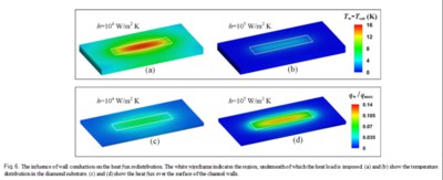
For flow evaporation in microchannels, the heat transfer coefficient is usually at the magnitude of 104–105 W/m2 K. We hence prescribe two different heat transfer coefficients of 104 and 105 W/m2 K, respectively, to see suggest the substrate can be cooled more effectively with increasing the heat transfer coefficient. The peak temperature always appears in the middle regions where the heat load is directly imposed. The ratio of the wall heat flux at the channel surface relative to the maximum imposed heat flux underneath the heat sink, is presented in Fig. 6(c) and (d). It can be seen that the heat flux is remarkably redistributed when it is conducted to the surface of channel walls due to the transverse wall conduction. Owning to this redistribution effect, the heat flux on the channel wall is greatly reduced down to less than 14% of the maximum imposed heat flux max. It is this significant heat flux redistribution effect that leads to a dramatic reduction of peak temperature in the solid. With the increase of the heat transfer coeffcient, the redistribution effect would be less significant because of the decrease of the convective heat resistance (white wireframe in Fig. 6(c and d)) as the heat transfer coefficient is increased. It is shown that the percentage of the heat flux concentrated in the directly heated zone, is increased with heat transfer coeffcient when h < 109 W/m2 K, whereas, above 109 W/m2 K, the heat flux percentage is no longer increased and remains constant at 73.36%. This is because the convective heat resistance is approximate to zero when heat transfer coefficient is infinitely large. This is attributed to the inherent existence of conductive heat resistance in the diamond substrate. This means the heat sink has a maximum cooling capacity that could control the mean temperature where is on the base of the directly heated region as low as Tc, and it is impossible to approach the saturation temperature of the refrigerant Tsat. Therefore, Tc corresponds to the maximum cooling capacity the system could achieve. For this reason, we define the cooling efficiency of the current system as:
how the heat transfer in the diamond substrate is influenced. The steady solutions are shown in Fig. 6. Fig. 6(a) and (b)

Here, we experimentally measured the cooling performance of a diamond made heat sink, with the saturated ammonia boiling undergoes in the V-shape channels. In subject to localized heat flux as high as 267 W/cm2, favorable cooling performance is achieved. The high efficiency is attribute to the diamond substrate could spread the heat flux transversely, and conse-quently, the heat flux at the channel wall is dramatically relaxed to a very low level. These combined effects pro-mote the cooling capacity of the heat sink dramatically, which are promising to manage even higher heat load.
CSMH focuses on the R&D and production of diamond wafers, and has created an efficient and precise machining method for diamond atomic-level surfaces based on plasma-assisted polishing, diamond wafer Ra<1nm, diamond heat sink thermal conductivity 1000-2000W/m.k, and GaN on diamond, Diamond on GaN, diamond-based aluminum nitride and other products. We will keep pursuing the innovation-driven development strategy in the future, offering our customers products of high quality and reliable performance while contributing the rapid development of the global semiconductor industry.
 闽ICP备2021005558号-1
Leave A Message