Pos:
Home KnowledgeTechnologyDiamond wafer application in a hybrid power module based on diamond and SiC devicesUnlike SiC unipolar devices, the on-state resistance of diamond unipolar devices based on bulk conduction has a negative temperature coefficient (NTC), reducing the conduction losses at high junction temperatures. Thus, to associate these opposed temperature coefficients, the current article focuses on modeling a hybrid power device composed of an n-type 4H-SiC MOSFET and a p-type diamond bulk FET device. The optimal performances and sizing of SiC and diamond devices are introduced and calculated, as an initial benchmark under the same specifications. Based on analytical modeling of both switching and conduction losses, junction
temperatures, and associated heatsink parameters, the hybrid device performances are evaluated for a synchronous buck converter operating at 1200 V-1 A and an ambient temperature of 300K. The results described in the manuscript highlight an equilibrium of the hybrid device total losses over a large range of temperatures as well as a reduction by two of the SiC active area. The proposed analysis could be further extended to different voltage/ current classes to meet the requirements of alternative applications.
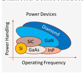
Diamond is an ultra-wide band gap semiconductor material, with a band gap of 5.5 EV, which is larger than that of Gan, SiC, and other wide band gap semiconductor materials. As shown in the following table, the band gap width of a diamond is 5 times that of the Si; The carrier mobility of the diamond is 3 times higher than that of the Si material. Theoretically, the carrier mobility of diamond is more than 2 times higher than that of existing wide band gap semiconductor materials (GaN and SiC). At the same time, diamond has extremely low intrinsic carrier concentration at room temperature. Besides the highest hardness, diamond also has the highest thermal conductivity among semiconductor materials, which is 7.5 times that of AlN. Therefore, diamond is also known as the "ultimate semiconductor" material in the industry.
CSMH is equipped with the most advanced MPCVD device to prepare large-area high-quality diamond films with high thickness uniformity and high growth rate. Special grinding and polishing equipment are used to make the surface roughness Ra of CVD diamond growth surface < 1 nm, with mirror-like luster. The thermal conductivity of the diamond heat sink is 1000-2000 W/ m.k.
Products include high quality diamond wafer, diamond heat sink, GaN & Diamond wafers, and PVD AlN template to provide you with the most complete diamond thermal management solution.

 闽ICP备2021005558号-1
Leave A Message