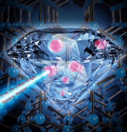
As a wide band-gap semiconductor, diamond possesses excellent physical and chemical properties and shows many attractive properties. For instance, it exhibits high electric-field breakdown strength, low dielectric constant, high thermal conductivity, and high transparency conductivity. Hole-doped diamond exhibits superconductivity at high pressure and temperature. Nanoscale single-crystalline and polycrystalline diamond needles exhibit ultra-large, fully reversible elastic deformation. It holds potential applications in the high-tech area, especially in those of high frequency, high temperature, and high-power electronic devices. Despite these interesting properties, the wide band gap of 5.5 eV and low electronic conductivity also limits its applications in electronic devices. And doping is regarded as the most popular method to tune its electronic and other relative properties. Diamond under doping has been studied extensively over the past decades. P-type doping in the diamond can be easily obtained by B doping. That is because the radius of the B atom is smaller than that of other atoms, and its solubility in diamond is high. Currently, great progress has been made in the research of B-doped p-type diamonds. Nevertheless, it is challenging to achieve an appropriate n-type diamond through doping, because a suitable donor is difficult to find. Many elements with n-type characteristics have been studied, such as Li, Na in group I, N, P in group V and O, S in group VI. However, interstitial Li or Na is insoluble and tends to form other impurities, which is unsuitable for realizing n-type diamonds. Substitutional N can denote an electron to the diamond, and then the deep donor level located at 1.4 eV below the conduction band edge can be found, which prevents it from being used in room-temperature semiconductor devices. P is a promising shallow donor candidate with a donor level of 0.43 eV below the conduction band edge. However, due to its low conductivities and carrier mobility, it is also unlikely to be used at room temperature. An n-type conducting layer creates an O-implanted diamond with activation energy is about 0.32 eV. But the oxygen donors become deactivated after being annealed above 600 °C. The preparation method of n-type diamond with reasonable quality is S doping, which shows a shallow donor level in the bandgap with the ionization energy of 0.38 eV and the electrons mobility of 597 cm2/Vs. Although good results have been obtained by S doping, it is difficult to be realized because of the quite low doping efficiency and solubility. Single-atom doped n-type diamonds cannot meet the requirements of semiconductor fabrication. To this end, co-doping strategies have been proposed for diamonds. For example, Miyazaki and his co-operator reported that the N-H-N complex in diamonds exhibits a much shallower donor character compared with an isolated N donor. Lombardi et al. systematically studied the interaction of H with B, P, and S in diamonds and found that it was energetically favorable for hydrogen to be trapped and to passivate boron and phosphorus. Li et al. revealed that co-doping B could enhance S doping in the diamond. The underlying physics for the B-S co-doping is also investigated based on theoretical calculations. Li et al. reported that the synergistic effect of B and N atoms made a lower Fermi energy, which could improve the conductivity significantly and promote the absorption edges shift to the visible-light region.
The heterostructure constructed by diamonds and other materials cannot only regulate the electronic properties of diamonds effectively, but also provide ideal platforms for other materials. In addition, diamond-composed heterostructures also hold great potential applications in photocatalysis, electronic devices, and other fields. However, a few works have been reported on diamond composite systems, which calls for further study.

CSMH is a joint venture company based on cutting-edge semiconductor manufacturing technologies with investments from Korea, China, and Singapore. We are equipped with advanced semiconductor production equipment to produce high-quality diamond wafer, diamond heat sinks and AlN templates on a variety of substrates, including AlN on Sapphire, AlN on Diamond, and AlN on Si. Our product's performance has improved to a level that is among the best in the world.
 闽ICP备2021005558号-1
Leave A Message