Gallium nitride (GaN) is hot. Even hotter is the race to integrate GaN with other materials to boost its performance.
A team led by the School of Mechanical Engineering at the Georgia Institute of Technology has reported a series of results using room-temperature surface-activated bonding (SAB) to bond GaN and single-crystal diamond with different interlayer thicknesses.1 The newly developed technique maximizes GaN’s performance for higher-power operation.
Integrating GaN with other materials is technically challenging. It’s difficult to bond diamond and GaN with thermally conductive interfaces and low stress at the interfaces. The new model allows GaN devices to take full advantage of the high thermal conductivity of single-crystal diamond and thus achieve an excellent cooling effect for high-power solutions. Because it is conducted at ambient temperatures, the process does not induce the physical stress problems that result from the different coefficients of thermal expansion for the materials used in other standard processes.
Silicon has reached its theoretical limit for power electronics. High-electron–mobility transistor (HEMT) devices based on GaN offer superior electrical characteristics and are a valid alternative to MOSFETs and IGBTs in high-voltage and high-switching-frequency motor control applications.
GaN is a wide-bandgap (WBG) material. As such, its forbidden band (corresponding to the energy required for an electron to pass from the valence band to the conduction band) is much wider than silicon’s: 3.4 electron-volts for GaN, compared with 1.12 eV for silicon. Because of this high required energy, the material thickness required for GaN to block a certain voltage is 10× thinner than silicon would require, enabling much more compact device sizes. The higher electron mobility of a GaN HEMT leads to a greater switching speed because the charges that normally accumulate in the joints can be dispersed more quickly. The faster rise times, lower drain-source on-resistance (RDS(on)) values, and reduced gate and output capacitance achievable with GaN all contribute to its low switching losses and ability to operate at switching frequencies up to 10× higher than silicon. Reducing power losses brings additional benefits, such as more efficient power distribution, less heat generation, and simpler cooling systems.
GaN performance and reliability are related to temperature and the Joule heating effect on the channel. Substrates such as silicon carbide (SiC) and diamond integrated into GaN can improve heat management, making it possible to lower the operating temperature of the device. For GaN-on-SiC devices, a 25° decrease in channel temperature would lead to about a 10× increase in device lifetime. As a result of these performance parameters, GaN devices have been deployed in optoelectronics, RF, and automotive applications. Target markets for GaN-on-diamond devices include defense radar and satellite communications, as well as the emerging market for 5G base stations.
Diamond’s thermal conductivity is 14× greater and its electrical field resistance 30× greater than silicon’s. High thermal conductivity allows the spreading of heat. Diamond has a bandgap of 5.47 eV, a breakdown field of 10 MV/cm, electron mobility of 2,200 cm2/Vs, and thermal conductivity of about 21 W/cmK.
Georgia Tech researchers collaborated on the new process with researchers from Meisei University and Waseda University. Their technique allows the placement of high-thermal-conductivity materials much closer to the regions of the active devices in gallium nitride, thus maximizing GaN performance for higher-power operations.

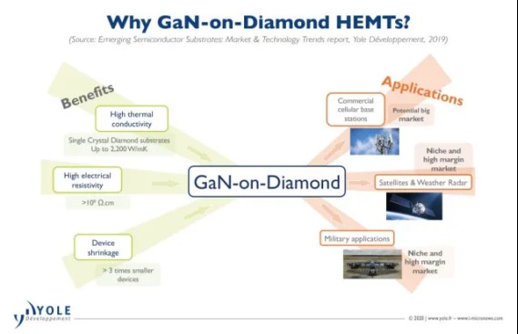
Figure 1: GaN-on-diamond applications overview
“GaN-on-diamond offers key parameters of high thermal conductivity, high electrical resistivity, and small form factor at both device and system level,” said Ezgi Dogmus, technology and market analyst at Yole Développement (Figure 1). “These benefits make GaN-on-diamond power amplifier devices very attractive for high-power RF applications, such as commercial base stations and military radar applications, as well as satellite communications and weather radars.”
Dogmus added that GaN-on-diamond has been in development for over a decade and is “expected to be launched commercially by leading industrial actors such as RFHIC, Akash Systems, and Mitsubishi Electric” in the coming years.
The maximum output power of GaN-based HEMTs is limited by the high temperature of the channel substrate, which degrades system performance and reliability. Diamond is currently the material with the highest thermal conductivity, and its integration with GaN helps to dissipate the heat generated near the channel.
“During HEMT device [operation], a large voltage drop near the gate induces localized Joule heating,” said Zhe Cheng, a recent Georgia Tech Ph.D. graduate who is the paper’s first author and now is a postdoctoral researcher at the University of Illinois Urbana-Champaign. “The heating area is located within tens of nanometers, which results in super-high local heat flux. The local heat flux value of GaN-based HEMTs could be more than 10× larger than that of the sun’s surface.
“Proper heat-spreading techniques, such as putting diamond as close as possible to the hot spots, could decrease the channel temperature effectively, facilitating the device stability and lifetime.” The techniques currently used involve the direct growth of diamond via chemical vapor deposition (CVD) on GaN with a dielectric as a protective layer because the plasmon during diamond growth would damage the GaN. The combination of the materials’ thermal resistance and the interfaces plays a pivotal role in heat flow management, especially for high-frequency applications for switching power supplies. With current techniques, the growth temperature of the CVD diamond exceeds 700°C. When the devices cool to room temperature, the stress at the interfaces would crack the wafers in the absence of an appropriate thermal management strategy. Additionally, the adhesion layer increases the thermal resistance of the GaN-diamond interface, which offsets the benefit of the diamond substrate’s high thermal conductivity.
The research presented by the team from Georgia Tech, Meisei University, and Waseda University used two modified SAB techniques to bond GaN with diamond substrates with different interlayers at room temperature. First, the two surfaces to be bonded were cleaned and activated by argon-ion beams, which generated dangling bonds at the surfaces. Then the two surfaces were pressed together at room temperature. The dangling bonds would form covalent bonds at the interfaces. Some silicon atoms were added at the interface to enhance the interfacial bonding. “The bonding is finished at Meisei University and Waseda University ([by] Fengwen Mu and Tadatomo Suga),” said Cheng. “Then the bonded interfaces are measured by time-domain thermo-reflectance (TDTR) at Georgia Tech ([by me], Luke Yates, and Samuel Graham). Related thermal modeling is also performed at Georgia Tech to evaluate the impact of the bonded interface on GaN devices.”
TDTR is used to measure thermal properties. Material characterization can be performed by high-resolution scanning transmission electron microscopy (HR-STEM) and electron energy loss spectroscopy (EELS).
Time-domain thermo-reflectance is a pump-probe technique performed with an ultra-fast femtosecond laser, which measures the thermal boundary conductance of the GaN-diamond interface. This technique uses an ultra-fast laser modulated between 1 and 12 MHz to control the thermal penetration depth. The probe pulse is delayed between 0.1 and 7 ns compared with the pump pulse to allow the decay of the relative surface temperature to be measured during the delay. A lock-in amplifier allows extraction of the read signal picked up by a photodetector. The temperature variation is measured by the reflectivity variations of a thin metal transducer (50 to 100 nm). The system is capable of measuring thermal conductivity between 0.1 and 1,000 W/mK and thermal boundary resistance between 2 and 500 m2K/G. A titanium-sapphire femtosecond laser is used.
In the work by Georgia Tech and its partners, GaN was bonded to diamond by adding silicon atoms at the interfaces to bolster the chemical adhesion of the interface and lower the thermal contact conductance. Thermal boundary conductance (TBC) is the heat conduction between solid-solid interfaces. The related coefficient is a property indicating the ability to conduct heat across interfaces.
The team used two samples. The first consisted of a thin layer of GaN (~700 nm) bonded on a commercial single-crystal diamond substrate (grown by CVD) with a silicon interlayer of ~10 nm in thickness. The second bonded a GaN thickness of ~1.88 μm on a commercial single-crystal diamond substrate grown by a high-pressure high-temperature (HPHT) method. The GaN was polished to be thin enough for TDTR measurements to be taken (Figures 2–4).
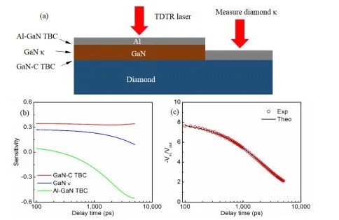
The thermal conductivity of the individual crystalline diamond substrates on the GaN-free area was measured, and then TDTR measurements were performed on the area with the GaN layer to measure the TBC of the GaN-diamond structure.
“The measured thermal conductivity of the diamond substrates was used as a known parameter in the adaptation of the TDTR data to extract the TBC when measuring above the GaN layer,” said Cheng. “Overall, there are three unknown parameters: Al-GaN TBC, GaN thermal conductivity, and GaN-diamond TBC.”

Figure 2: (a) TDTR measurements on the diamond and bonded GaN-diamond samples. (b) TDTR sensitivity of the three unknown parameters. (c) TDTR data fitting of Samp2 with a modulation frequency of 2.2 MHz at room temperature

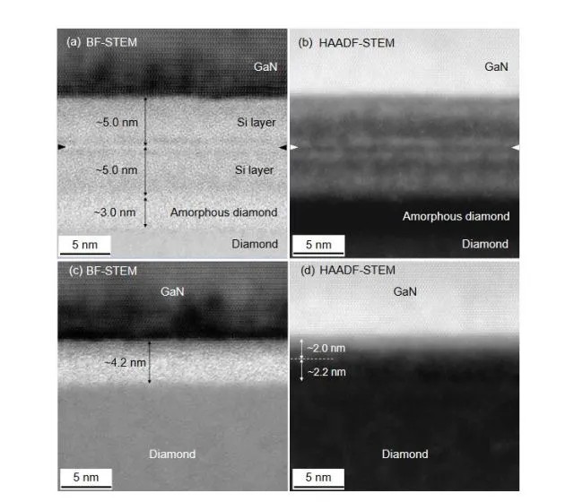
Figure 3: (a-b) Cross-section images of GaN-diamond interfaces of Sample 1. (c-d) Cross-section images of GaN-diamond interfaces of Sample 2.
The TBC measurements of GaN-diamond interfaces are among the high values reported in scientific literature and are influenced by the thickness of the interlayer. Because of the disorder and defects of the interfaces, weak temperature dependence traditionally has been observed for GaN-on-diamond. The new model shows a relatively large GaN-on-diamond TBC (>50 MW/m2K). This could allow the high thermal conductivity of the single crystalline diamond to be fully used.
 闽ICP备2021005558号-1
Leave A Message