Pos:
Home KnowledgeTechnologyResearch on the Electrical Properties of Boron-Doped Single-Crystal DiamondDiamond exhibits excellent electrical properties, including a wide band gap and high carrier mobility. Intrinsic CVD diamond films are good insulating materials with a resistivity of up to 10¹⁶ Ω·cm, which are almost non-conductive at room temperature, limiting their applications in electronics. Doping can transform diamond from an insulator into a semiconductor, conductor, or even a superconductor. P-type diamond is generally obtained by doping elements of the 13th group of the periodic table. Among them, boron atoms, with a radius close to that of carbon atoms composing diamond, can be easily doped into diamond to replace carbon atoms and introduce a shallow acceptor level (approximately 0.37 eV). This endows boron-doped diamond films with well-conductive p-type semiconductor characteristics at room temperature, expanding their electrical applications. Heavy boron-doped diamond films prepared by the MPCVD method were studied for their superconducting properties, revealing a transition temperature of 7.4 K and a zero-resistance temperature of 4.2 K.

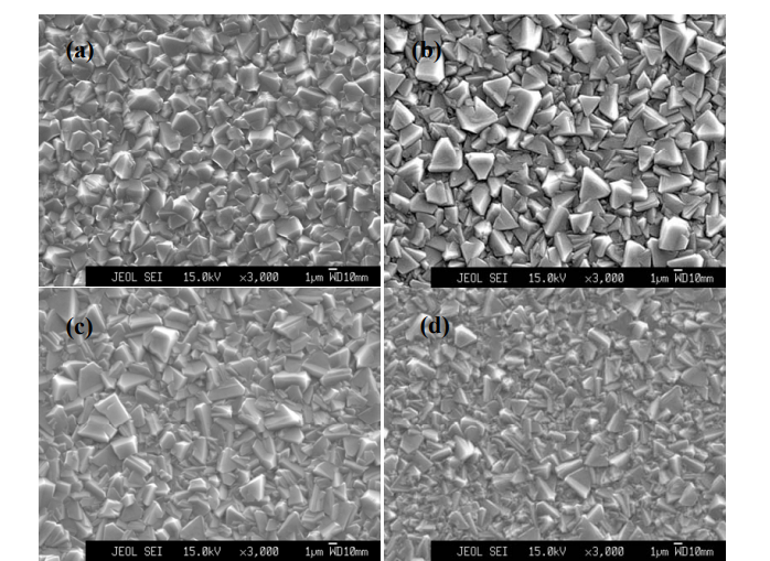
Studies have shown that the incorporation of a small amount of boron is beneficial for improving the quality of diamond; however, as the boron concentration continues to increase to a certain level, the film quality decreases instead. Both the grain size and growth rate of boron-doped diamond follow a pattern of first increasing and then decreasing with the rise in boron concentration. The reason for this phenomenon is analyzed as follows: the introduction of a small amount of boron enhances the activity of carbon-containing groups on the substrate surface, thereby promoting the growth of diamond films. In contrast, the presence of excessive boron disrupts the growth atmosphere and crystal structure of diamond, ultimately inhibiting the growth of diamond films and reducing their quality.
XRD results of boron-doped diamond films indicate that boron incorporation causes diamond to exhibit more (111) crystal planes while suppressing the growth of other crystal planes. Raman spectroscopy analysis reveals that a small amount of boron helps improve the quality of diamond films. As the boron concentration further increases, new peaks appear at low wavenumbers of 520 cm⁻¹ and 1200 cm⁻¹ due to lattice distortion caused by boron doping. Meanwhile, the characteristic peak of diamond begins to shift toward lower wavenumbers and shows asymmetry, a phenomenon that can be explained by the Fano effect.
Hall effect measurements demonstrate that the prepared boron-doped diamond possesses relatively excellent electrical properties. When the boron flow rate is 4 sccm, the resistivity of the film reaches nearly 10⁻³ Ω·cm. The carrier concentration reaches 10¹⁸ cm⁻³ when the boron flow rate is 2 sccm and increases continuously with the rise in boron concentration. Due to the high nucleation density, low growth rate, small grain size of the prepared boron-doped diamond films, the grain boundary density on the film surface is very high. There are numerous traps near these grain boundaries, which easily capture carriers and form a large number of potential barrier regions. These potential barrier regions hinder the movement of carriers; additionally, the scattering probability of impurities in the film increases with the increase in boron concentration. Therefore, the Hall mobility of all boron-doped diamond films with different boron contents is lower than 5 cm²·V⁻¹·s⁻¹, which is much smaller than the mobility of single-crystal diamond.
The boron-doped single-crystal diamond produced by CSMH can achieve doping from low concentration to high concentration. It has realized a uniform and controllable concentration and a customizable boron doping process.CSMH uses the MPCVD method to prepare large-sized and high-quality diamonds,and currently has mature products such as diamond heat sinks, diamond wafers, diamond windows,diamond hetero junction integrated composite substrates,etc.
 闽ICP备2021005558号-1
Leave A Message