Diamond is hailed as the "ultimate semiconductor material," boasting the highest thermal conductivity among all semiconductors, along with an extremely high breakdown electric field, extremely high carrier mobility, an ultra-wide bandgap, and excellent radiation resistance.

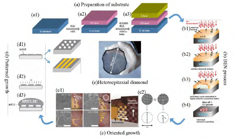
Currently, the preparation technologies for large-size single-crystal diamond wafers mainly include homoepitaxial growth, mosaic stitching, and heteroepitaxial growth. Through methods such as high-energy particle bombardment, stitching growth, and growth with buffer layers on other substrates, the large-size preparation of single-crystal diamond wafers can be achieved.
With its ultimate heat dissipation solution, diamond wafers can accelerate silicon chips—it can build a "thermal highway" within atomic distances of the transistors in chips operating at high intensity, dissipating heat with ideal efficiency, reducing hotspots, and thereby tripling the computing speed of the chips.
Moreover, diamond wafers possess both extreme thermal conductivity and electrical insulation properties, which enable new architectures to achieve fundamental breakthroughs in miniaturization, efficiency, and robustness.
In the field of wireless communication, diamond wafers can also form an "ultimate semiconductor sandwich" with gallium nitride (GaN) semiconductors. GaN semiconductors power a growing number of high-performance wireless communication devices, and diamond wafers, by addressing the overheating and voltage issues faced by GaN, allow GaN to outperform silicon carbide in all indicators.
CSMH uses the MPCVD method to prepare large-sized and high-quality diamonds,and currently has mature products such as diamond heat sinks, diamond wafers, diamond windows,diamond hetero junction integrated composite substrates,etc.Among them,the thermal conductivity of diamond heat sinks is 1000-2200w/(m.k), and the surface roughness of diamond wafer a<1nm.It has been applied in aerospace, high-power semiconductor lasers, optical communication, chip heat dissipation, nuclear fusion and other fields.
 闽ICP备2021005558号-1
Leave A Message