Pos:
Home KnowledgeTechnologyDiamond Wafer as the heat spreader for the thermal dissipation of GaN-based electronic devicesWith the increased power density, self-heating inside the devices becomes an essential issue that accelerates the failure and poor reliability in the real application. Thermal dissipation through conventionally used approaches is no longer adequate. To achieve the effective thermal dissipation, the heat spreader with a much higher thermal conductivity is required. The ideal heat spreader would be a substrate that is both highly thermally conductive and electrically insulating. Diamond, with the thermal conductivity up to 2400W/mK at room temperature for the single crystals, and approaching 2000W/ mK for the polycrystals, is the best candidate as a heat spreader for GaN power transistors.
Over the past twenty years, a variety of methods have been developed to utilize diamond as the heat spreader for AlGaN/GaN power transistors. The developed wafer is therefore called “GaN-on-diamond wafer”. For the approaches, the thermal resistance at the GaN/diamond, which is referred to the “effective thermal boundary resistance (TBReff)”, is one of the factors that significantly increases the overall temperatures during device operation. Therefore, the optimizations on the integration technique and interface property are important. Then we will present the state-of-the-art development on the GaN-on-diamond wafer and the modified fabrication process for HEMTs with regard to different integration methods.
The advantage for the GaN bonding to diamond is that the crystal quality of both GaN and diamond can be guaranteed after the bonding. The formation of GaN-on-diamond wafer started with GaN or AlGaN/GaN HEMT epitaxial layers grown on a silicon substrate. Other substrates, such as sapphire, silicon carbide, or aluminum nitride may also be used. The GaNon-diamond wafer technology has been demonstrated with 80 to 100µm thick diamond substrates, which are mechanically stronger and flatter than that of the thin wafers. The developed GaN-on-diamond substrates were then utilized for the fabrication of devices, which demonstrated transition frequencies up to 85GHz.

The nano-crystalline and poly-crystalline diamond were also proposed as the template for the epitaxial growth of GaN to achieve the effective thermal dissipation. The diamond was firstly deposited on the silicon substrate, therefore, there is no limitation in the substrate size. A low-temperature buffer layer is typically utilized before the deposition of GaN films. Unfortunately, the GaN layer was not pure wurtzite structure and the polycrystalline form was typically observed. An epitaxial lateral overgrowth (ELO) of single-crystalline thick GaN films were reported on the polycrystalline diamond. The polycrystalline diamond was deposited on the GaN/Si wafers using hot filament CVD. The GaN was grown on the window region between the diamond stripes. A lower pressure, higher V/III ratio, higher temperature, and GaN window mask openings along [11̅00] resulted in enhanced lateral growth of GaN. Complete lateral coverage and coalescence of GaN were achieved over a [11̅00]-oriented 5μm-wide GaN window between 5μm diamond stripes.
The uniqueness of the direct CVD diamond growth on GaN is that the diamond can be deposited as close as possible to the Joule heating location of the HEMTs. This approach is highly effective for the thermal dissipation of HEMTs. However, it has limitations that restrict this technique. The interface thermal properties between GaN and NCD diamond were improved by Smith et al. using a two-step mixed-seeding method. While the diamond directly grown onto GaN was proved to be unsuccessful due to the poor adhesion. The two-step mixed-seeding method gave TBReff values lower than 6m2 K/GW, 30 times smaller than those of films using nanodiamond seeding alone. Such remarkably low thermal barriers obtained with the mixed-seeding process of microdiamond and nanodiamond offer a promising route for the fabrication of high-power GaN HEMTs using diamond as a heat spreader. The double-side diamond integration to the HEMTs devices were also developed to improve the heat dissipation. In 2019, Fujitsu Limited and Fujitsu Laboratories Ltd. deposited diamond films on the front surface of the HEMT device. They also bonded the SCD on the back side of HEMTs using SiC interlayer, as shown in Figure 13 [89]. The nanodiamond films were grown at a temperature of 650 °C without degrading the transistors’ performance. With the NCD layer on the front side, the amount of heat generated during HEMT operation was reduced by approximately 40% compared to that without the diamond film, and the temperature can be lowered by 100 °C or more. By combining the heat dissipation from the back side of the GaN HEMT with SCD substrate, the operating temperature is expected to be reduced by approximately 77%.
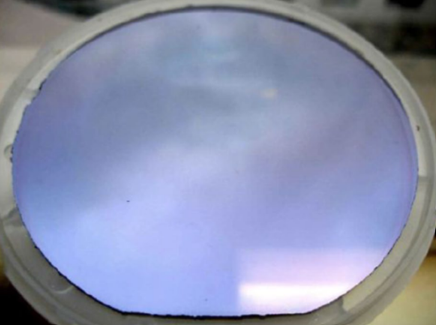
CSMH has made breakthroughs in GaN & Diamond combination solutions: GaN on Diamond Diamond on GaN, and GaN & Diamond bonding. Among them, the required diamond wafer's performance has improved to a level that is among the best in the world with Ra<1nm (even <0.5nm). We also supply high quality polycrystaline diamond wafer, diamond heat sink, diamond window etc.
 闽ICP备2021005558号-1
Leave A Message