High power light emitting diodes (LEDs) have become the main light source in every day applications. These compact devices have a large lighting capability and spend only a fraction of the energy required to power filament bulbs, nevertheless self-heating is one of the most limiting issues of power LEDs. LEDs do not emit IR radiation directly, however, at high levels of current, ohmic losses in the parasitic resistances of contacts and cladding layers cannot be neglected and it is estimated that 75% of the electric power is converted into heat . The LED die is typically encapsulated inside a dome-shaped material with a large refractive index. This dome improves the extraction of light from the device; however, dome materials are also poor conductors of heat, which creates an additional issue since convection may no longer be used to remove the heat away from the junction. Both LED manufacturers and circuit designers have come up with a variety of creative strategies to carry the heat away of the junction and guarantee that the junction temperature TJ remains as low as possible during device operation.

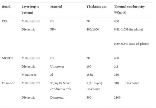
Structure, dimensions, and thermal conductivity (λ) of the different boards layers.
Thanks to properties such as high bandgap (5.4eV), breakdown electric field (2×10⁷V/cm), and λ (1800–2000W/(m·K) , diamond comes as a candidate to improve the thermal management of power devices. The use of diamond as a HS has been proposed in 1967; in comparison with regular Cu HSs, its use doubled the continuous power density of Si avalanche diodes . Diamond has also been used to improve the thermal management of power LEDs at different levels. Horng et al. mounted the LED die on an aluminium (Al) board coated with a diamond-like layer and obtained an 11°C reduction in TJ at 350mA in comparison to mounting the LED on a conventional MCPCB. Chen et al. reported a 20°C reduction in TJ at 1 A when the LED chips were bonded to Si substrates coated with 20μm of diamond. Fan et al. replaced the Cu HS of white power LEDs with a diamond/Cu composite material and the weight of the internal HS was reduced by more than 35%; simultaneously the thermal resistance and TJ decreased 10.5% and 33.3%, respectively. Diamond films have also been integrated in grooves etched on the upper ITO layer of LEDs. The replacement of the AlN carrier of Cree XLamp XB-D LEDs with a diamond plate is estimated to improve the lifetime of the devices by 25% and 50% for 350 (nominal current) and 800mA, respectively, and to decrease the drift of the wavelength with the current level .

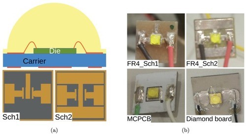
(a, top) LED cross-section view (drawing not to scale). (a, bottom) Electrodes layout. LEDs mounted on different boards(b, top) FR4 boards (electrode layout Sch1 and Sch2) and (b, bottom) MCPCB/diamond boards (electrode layout Sch1).
On the other hand, the MTTF increases significantly when the LED is mounted on the diamond board (in comparison with the MCPCB). For the lowest Ea, MTTF increases 60/80% for a current of 350/700mA. For 2.5eV, the AF is as low as 0.11/0.03 (350/700mA). If mounted on the diamond board, the LED could be operated at 700mA – and this would have a negligible impact in comparison to the MTTF of a similar LED mounted on a MCPCB and operated at 350mA. In addition,Diamond plates feature a very low coefficient of thermal expansion (CTE, 1×10⁻⁶/°C at room temperature),this is an advantage, since diamond boards show a greater dimensional stability than common FR4 boards (with CTE=9.2×10⁻⁶/°C).
These results show that, for highly demanding applications in terms of power/lifetime, the use of diamond boards should be considered. Therefore, for high end applications – such as the case of the space industry – the use of diamond boards can bring an additional advantage. An example is the development and commercialization of the GaN-on-diamond technology to fabricate HEMTs and power amplifiers, radio, and transmitter modules for space satellites by Qorvo and Akash Systems. In the GaN-on-diamond technology the diamond is integrated at the wafer level.
The junction temperature of Cree cold white XLamp XB-D LEDs mounted on 1cm2 FR4, MCPCB, and diamond boards was measured for different current ratings. The experimental results were additionally validated with an analytical thermal model. Compared with the MCPCBs commonly used to mount power LEDs, FR4 boards show a much poorer thermal performance, as expected; in the worst case, and taking as a reference the MCPCB board, the junction temperature increases ≃34 and ≃72°C for 350 and 700mA forward current, respectively. The replacement of the MCPCB with diamond decreases the junction temperature, for the same current levels, ≃19 and ≃24°C, respectively. The variation in the junction temperature has a tremendous impact on the lifetime of the LEDs. Depending on the activation energy of the aging processes, LEDs mounted on the diamond board will age 60–90% slower for 350mA forward current and 90–99% slower for 700mA, in comparison with those mounted on the MCPCB. There results show the potential of using diamond boards.
The technical indicators of the existing diamond heat sinks and diamond wafer products of CSMH have reached the world's leading level. The surface roughness of the diamond wafer growth surface is Ra<1nm, and the thermal conductivity of the diamond heat sinks reaches 1000-2000W/m . High-power semiconductor lasers using diamond heat sinks have been used in optical communications, and are also used in laser diodes, LED light-emitting diodes, power transistors, electronic packaging materials and other fields. Based on wafer-level diamond product capabilities, the company has developed GaN-on-diamond epitaxial wafers, which are mainly used in radio frequency (satellite, 5G base station) and high-power devices (photovoltaic, wind power, new energy vehicles, energy storage) and other Areas with high thermal management needs, as a complement to GaN-on-SiC materials.
 闽ICP备2021005558号-1
Leave A Message