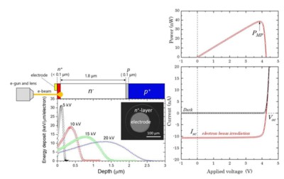
Diamond is an ultra-wide gap (5.5 ev) semiconducting material which has several ideal properties for radiation detectors, such as solar blindness, high-temperature operation, and fast response. Furthermore, diamond has near tissue equivalence due to its low atomic number (Z = 6) and chemical stability due to its strong covalent bonds. Because of these features, diamond has long been used as a radiation detector in the fields of nuclear engineering, nuclear fusion, high energy physics, and medical therapy. Until the 1990s, most of the research was conducted using selected high purity natural diamonds. Since the 2000s, the detector characteristics of synthetic diamond detectors have been greatly improved by achieving high purity diamond by microwave plasma enhanced chemical vapor deposition (CVD). Single-crystal CVD diamonds present the best characteristics for spectroscopy in diamond radiation detectors. For applications requiring large sensitive areas, polycrystalline CVD diamond is mostly used. Heteroepitaxial diamond detectors are a promising alternative to increase the area of spectroscopic diamond radiation detectors. For applications in extreme environments, high radiation flux which leads to polarization effects is a crucial issue. even with diamond, which has excellent radiation hardness, degradation of detector characteristics due to irradiation is inevitable. Detectors designed with small carrier travel distances, such as membrane diamond detectors and three-dimensional diamond radiation detectors, are effective ways to mitigate the degradation.
The properties of diamond radiation detectors are described by mobility and carrier lifetime. These characteristics are affected by temperature, defects, and impurities. In particular, impurities strongly affect the carrier transport characteristics in the detectors. Improvements in microwave-enhanced CVD diamond growth technology have led to ultra-high purity diamond crystals. These single crystal diamond radiation detectors showed ideal charge collection efficiency and energy resolution under irradiation conditions with low count rates at room temperature. Different types of crystals and detector structures are required to depend on purposes. For energy spectroscopy applications with a small area, a single crystal diamond is used. Polycrystalline diamond can cover a large area and is used for timing and position detection. Heteroepitaxial diamond has been shown to have characteristics similar to those of single crystal for hole drift mode. It may offer a larger detection area for spectroscopy than single-crystal diamond. Moreover, the size of the single-crystal diamond wafer has also been increasing in recent years due to the realization of mosaic diamond wafer and the progress of HPHT diamond growth technology. Though the most common detector is the planar structure, concepts such as thin-film type and three-dimensional structure have been proposed, which present operation with lower bias voltages than conventional planar-type detectors and improves radiation hardness by reducing charge travel distance in the detector. One of the promising fields for use of diamond radiation detectors is in harsh environments. Compared with other wide-gap materials, diamond has a particular advantage in high-temperature operation. Operation at temperatures close to 500 °C has been confirmed for diamond radiation detectors and MESFETs. In addition to detectors and FETs, it is also required to develop discrete devices which withstand harsh environments.
CSMH is a joint venture company based on cutting-edge semiconductor manufacturing technologies with investments from Korea, China, and Singapore. We have carried out cooperation with Asia University and the Semiconductor Research Institute of Jimei University; Initiated by the top scientists in the global semiconductor field to establish a research and development platform; Bringing together a large number of senior engineers of Diamond wafer, Diamond heat sinks and AIN materials;
Possess a substantial intellectual property (IP) portfolio;
Has two R&D bases in China and South Korea;
Won the title of "Xiamen Key Laboratory of Ultra Wide Bandgap Semiconductor Materials and Devices".

 闽ICP备2021005558号-1
Leave A Message