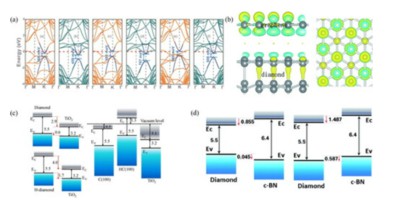
Diamond is widely used in semiconductor devices due to its excellent mechanical and optoelectronic properties. Plenty of approaches have been performed to tune its electronic properties due to the large bandgap, including doping, constructing heterostructure, and so on. The synthesis and application of p-type diamond with B as the impurity element are relatively mature, and the impurity level and carrier transport properties can be well controlled by research using ion implantation or the CVD method. However, the lack of effective n-type conductive diamond materials limits the application of diamonds in the field of electronics devices.
In recent years, a lot of theoretical and experimental works have been performed in the field of n-type diamond materials. The doping mechanism and effective doping methods of group I elements, mainly Li and Na, are seldom reported at present and need to be further discussed. Group V elements are used as donor impurities for N and P. However, a diamond doped with N does not show the characteristics of an N-type diamond at room temperature. Compared with N, P shows a better index and is regarded as an ideal donor impurity. Unfortunately, substances containing P are often highly toxic, which limits their further application. As for group VI elements, S impurity is more ideal than O, but the electron mobility is not high enough. Therefore, it is difficult to prepare n-type diamond films with low resistivity based on a single element. The possibility of co-doping in diamonds has been preliminarily explored through different methods. Experiments have proved that the co-doping of B, S or B, P atoms can not only improve the mobility, lattice integrity, and the solubility of a donor impurity in diamond but also can reduce the ionization activation energy of diamond. However, the study of electrical properties of co-doped n-type diamond semiconductors needs to be further improved.
On the other hand, heterostructure materials constructed by diamond-based materials also show their great application potential in electronic devices. Such materials can not only be used as substrate materials but also unveil promising applications in field-effect transistors and high-power electronic devices.

CSMH focuses on the R&D and production of CVD diamond wafers, and has created an efficient and precise machining method for diamond atomic-level surfaces based on plasma-assisted polishing, diamond wafer Ra<1nm, diamond heat sink thermal conductivity 1000-2000W/m.k, and GaN on diamond, Diamond on GaN, diamond-based aluminum nitride and other products. We will keep pursuing the innovation-driven development strategy in the future, offering our customers products of high quality and reliable performance while contributing the rapid development of the global semiconductor industry.
 闽ICP备2021005558号-1
Leave A Message